

Page 1
Ordering number: EN 4528B
Monolithic Digital IC
LB1643
Forward/Reverse Motor Driver with Brake
Overview
The LB1643 is a forward/reverse motor driver IC. The
direction and brake functions are controlled from a single
input, and the output voltages can be set by resistors. Further,
the output voltage has 3 modes, full, high-level and low-level
voltage modes. The output voltage can be controlled from a
single input and a microcontroller interface.
Features
.
Single-input forward, reverse and brake functions
.
Output voltage can be set using resistors
.
Single-input full-drive, high-level drive and low-level drive
select function
.
Microcontroller interface
.
Built-in surge-current absorption components
.
Built-in reference voltage circuit
.
Built-in thermal protection circuit
Specifications
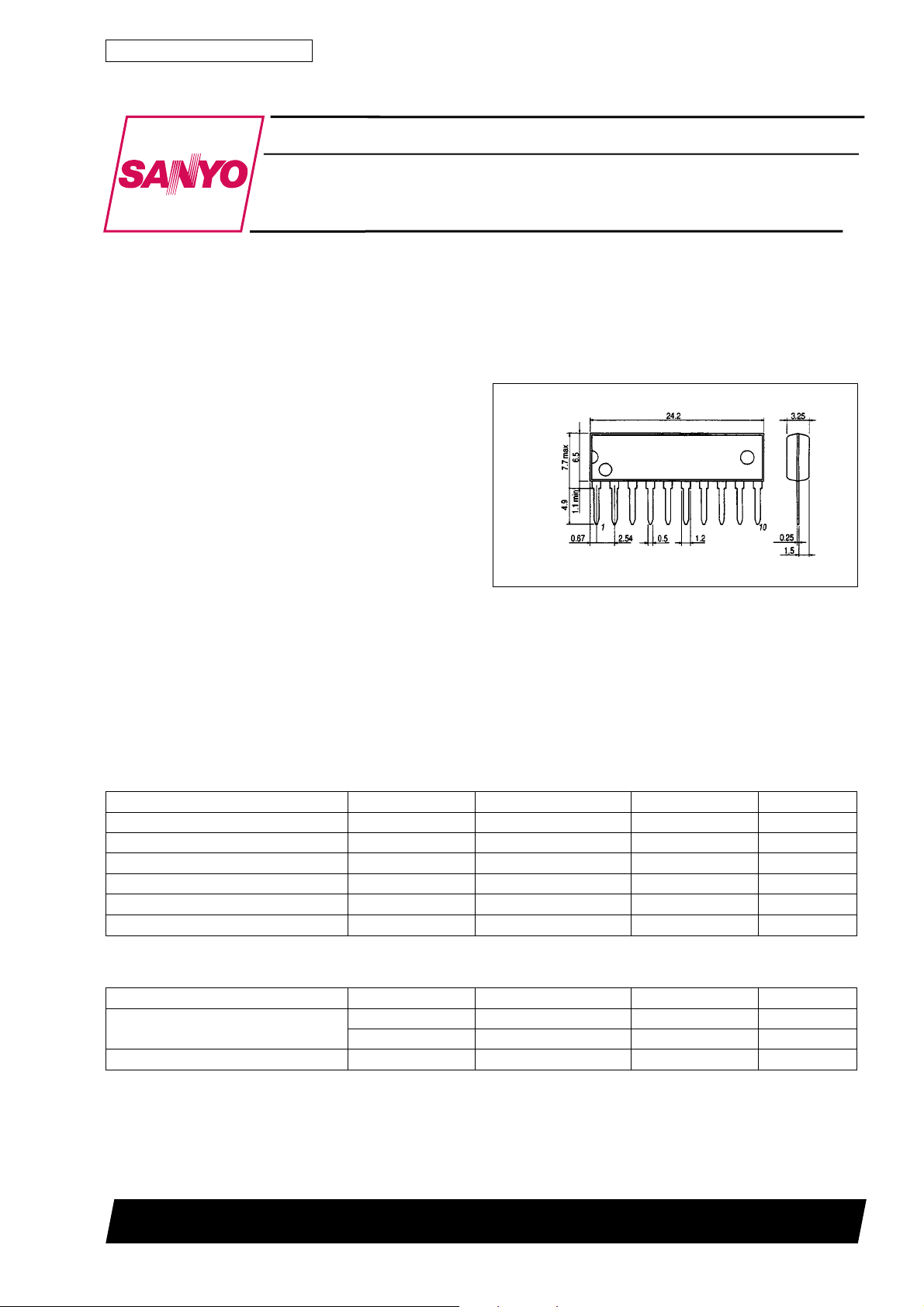
Package Dimensions
unit : mm
3043A-SIP10
[LB1643]
SANYO : SIP10
Absolute Maximum Ratings atTa=25°C
Parameter Symbol Conditions Ratings Unit
Maximum supply voltage V
Input voltage V
Output current I
Allowable power dissipation Pd max 1.2 W
Operating temperature Topr –25 to +75
Storage temperature Tstg –55 to +125
max 18 V
CC
IN
OUT
VCC> V
IN
–0.3 to +6 V
±1.6 A
Allowable Operating Ranges atTa=25°C
Parameter Symbol Conditions Ratings Unit
V
1 8.0 to 18 V
Supply voltage ranges
Forward-reverse direction prohibit time t off ^20 µs
CC
V
2V
CC
CC1
^ V
CC2
5to18 V
SANYO Electric Co.,Ltd. Semiconductor Bussiness Headquarters
TOKYO OFFICE Tokyo Bldg., 1-10, 1 Chome, Ueno, Taito-ku, TOKYO, 110-8534 JAPAN
63098HA(II)/D2293TS B8-0434 No.4528-1/5
C
°
C
°
Page 2
LB1643
Electrical Characteristics atTa=25°C, VCC=12V
Parameter Symbol Conditions min typ max Unit
Input low-level voltage V
Input high-level voltage V
Input mid-level voltage V
Input impedance Z
Current drain I
Output voltages
Output leakage current I
Saturation voltages (upper)
Saturation voltages (lower)
Reference voltage Vref 6.0 6.35 6.8 V
Reference voltage load
characteristics
Control to output gain
Thermal shutdown temperature T
INL
INH
INM
IN
CC
V
OUT1
V
OUT2
OL
Vsat11 V
Vsat12 V
Vsat21 V
Vsat22 V
∆Vref
∆Iref
TSD
RL=60Ω,VCH= 2.5 V, VIN1 = 2.5 V, VIN2 = 0 V 4.4 4.95 5.4 V
RL=60Ω,VCH= 2.5 V, VIN1 = 2.5 V, VIN2 = 5.0 V 4.4 4.95 5.4 V
RL= ∞ 0.01 1.0 mA
=12V,I
CC
=12V,I
CC
=12V,I
CC
=12V,I
CC
Iref = –2.0 to 0 mA 0.05 0.1 V/mA
V
OUT/VCH,VOUT/VCL
VCH= 2.5 V, VCL= 2.5 V, RL=60Ω
See note. 150 180
= 300 mA 1.9 2.2 V
OUT
= 500 mA 1.9 2.3 V
OUT
= 300 mA 0.25 0.5 V
OUT
= 500 mA 0.4 0.65 V
OUT
Note: Design target value only (not measured).
0 1.0 V
4.2 6.0 V
2.0 3.0 V
75 kΩ
5.5 10 mA
1.5 1.9 2.4 Times
C
°
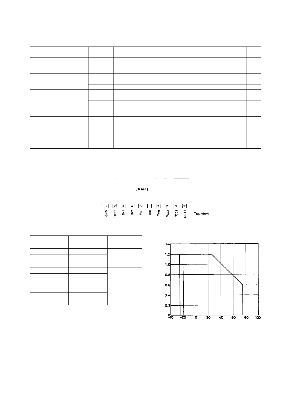
Pin Assignment
Truth Table
Input Output voltage
IN1 IN2 OUT1 OUT2
H H L FULL
LHL2V
H M OFF OFF
L M OFF OFF
H L FULL LOW
LOW
LOW
LL2V
Input levels are
.
VH^ 4.2 V
.
VM= 2.0 to 3.0 V
.
VL% 1.0 V
CH
CL
CH
CL
Forward (reverse)MHL2V
Reverse (forward)ML2V
Operation
BrakeM M OFF OFF
Allowable power dissipation, Pd max – mW
Pd max – Ta
Ambient temperature, Ta –°C
When IN1 and IN2 are open, they take on a voltage of 2.5 V.
Operation equivalent to LB1641.
No. 4528-2/5
Page 3

Internal Equivalent Circuit
Logic circuit
LB1643
Pre-driver
Thermal
protection circuit
Reference
voltage circuit
Sample Application Circuit
Motor
Microcontroller ports
Usage Notes
1. Use a microcontroller with CMOS output ports for hight-level, low-level and open-circuit conditions.
2. It is recommended that R1, R2 and R3 total approximately 60 kΩ.
3. The input voltage for IN1 and IN2 should be 0 to 6 V to ensure the output voltage does not cause incorrect operation when a
negative voltage is applied. Furthermore, IN1 and IN2 voltages should not be applied if the V
4. To avoid occurrences where both the upper and lower transistors are ON simultaneously, make sure IN1 or IN2 is open for a
period of tens of ms before switching control to the opposite device.
5. Connect a 20 µF or larger capacitor between V
and GND.
CC
6. A large current of several hundred mA flows in the motor circuits when the motor is being driven. Accordingly, the output
current line and the input circuit should be wired so that they do not have a common impedance.
supply is not applied.
CC
PS No. 4528-3/5
Page 4

LB1643
Pin Description
Pin No. Pin name Equivalent circuit Description
1 GND
3 IN1
4 IN2
.
Power and signal ground
.
Output voltage control input terminal
.
VM≅ 2.5 V when input is open.
.
Forward, reverse and brake control input
terminal
.
VM≅ 2.5 V when input is open.
5V
6V
7 Vref
CL
CH
.
Output voltage set terminal
.
Output voltage set terminal
.
Reference voltage output. Vref = 6.35 V
8V
9V
CC
CC
1
2
.
Signal voltage supply
.
Power voltage supply
No. 4528-4/5
Page 5

LB1643
Pin No. Pin name Equivalent circuit Description
2 OUT1
.
Motor coil connection terminals
10 OUT2
No products described or contained herein are intended for use in surgical implants, life-support systems,
aerospace equipment, nuclear power control systems, vehicles, disaster/crime-prevention equipment and the like,
the failure of which may directly or indirectly cause injury, death or property loss.
Anyone purchasing any products described or contained herein for an above-mentioned use shall:
1 Accept full responsibility and indemnifyanddefend SANYO ELECTRIC CO., LTD., its affiliates,subsidiariesand
distributors and all their officers and employees, jointly and severally, against any and all claims and litigation
and all damages, cost and expenses associated with such use:
2 Not impose any responsibility for any fault or negligence which may be cited in any such claim or litigation on
SANYO ELECTRIC CO., LTD., its affiliates, subsidiaries and distributors or any of their officers and employees
jointly or severally.
Information (including circuit diagrams and circuit parameters) herein is for example only; it is not guaranteed for
volume production. SANYO believes information herein is accurate and reliable, but no guarantees are made or
implied regarding its use or any infringements of intellectual property rights or other rights of third parties.
This catalog provides information as of June, 1998. Specifications and information herein are subject to change without notice.
PS No. 4528-5/5
 Loading...