

Page 1
Any and all SANYO products described or contained herein do not have specifications that can handle
applications that require extremely high levels of reliability, such as life-support systems, aircraft’s
control systems, or other applications whose failure can be reasonably expected to result in serious
physical and/or material damage. Consult with your SANYO representative nearest you before using
any SANYO products described or contained herein in such applications.
SANYO assumes no responsibility for equipment failures that result from using products at values that
exceed, even momentarily, rated values (such as maximum ratings, operating condition ranges,or other
parameters) listed in products specifications of any and all SANYO products described or contained
herein.
Monolithic Digital IC
3-Phase Brushless Motor Driver
Ordering number:ENN3323
LB1619M
SANYO Electric Co.,Ltd. Semiconductor Company
TOKYO OFFICE Tokyo Bldg., 1-10, 1 Chome, Ueno, Taito-ku, TOKYO, 110-8534 JAPAN
Applications
The LB1619M is a 3-phase brushless motor driver IC ideally suited for use in VCR capstan motor driver, drum mo-
tor driver applications.
Features
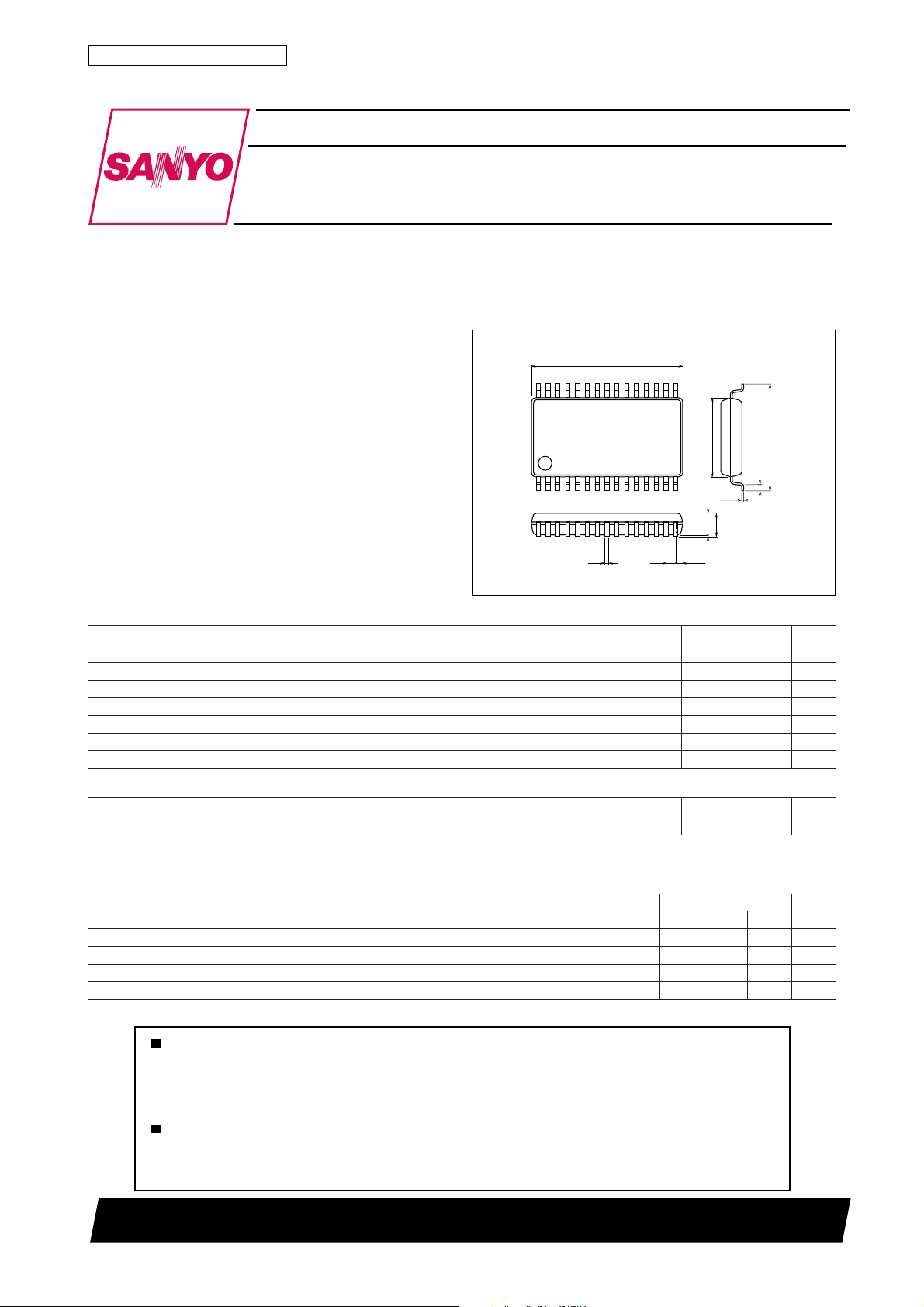
Package Dimensions
unit:mm
3073B-MFP30SD
[LB1619M]
15.2
30
• 120° voltage linear type.
• Speed control based on motor voltage control.
• Soft switching type eliminating noises caused by current
switching and making the values of external capacitors
smaller (comparable to those of chip capacitors).
• On-chip torque ripple compensation circuit.
1
• On-chip thermal shutdown circuit.
0.4
Specifications
Absolute Maximum Ratings at Ta = 25˚C
retemaraPlobmySsnoitidnoCsgnitaRtinU
egatlovylppusmumixaMV
egatlovylppusmumixaMV
tnerructuptuOI
tnerrucylppusllaHI
noitapissidrewopelbawollAxamdP 0.1W
erutarepmetgnitarepOrpoT 57+ot02–
erutarepmetegarotSgtsT 521+ot55–
Allowable Operating Ranges at Ta = 25˚C
retemaraPlobmySsnoitidnoCsgnitaRtinU
egatlovylppuSV
(Design Notes) It should be noted that dielectric breakdown is liable to occur between pin 11 and other pins.
xam 61V
CC
xam V
S
O
H
CC
16
0.25
2.45max
9.2
10.5
0.65
V
CC
5.1A
02Am
˚C
˚C
61ot6V
7.9
15
(2.25)
0.1
(0.6)
1.0
SANYO : MFP30SD
Electrical Characteristics at Ta = 25˚C, VCC=12V, VS=3V
retemaraPlobmySsnoitidnoC
1tnerrucylppuSI
2tnerrucylppuSI
tnerrucybdnatsylppuSI
egatlovnoitarutastuptuOV
VRBV5=8132Am
CC
VRBV5=0.50.7Am
S
V
QOCC
I
)tas(O
V0=081Aµ
YBTS
TUO
ecruos+knis,A0.1= 3.2V
22801TN (KT)/3270YT, TS No.3323–1/7
sgnitaR
nimpytxam
Continued on next page.
tinU
Page 2
LB1619M
Continued from preceding page.
retemaraPlobmySsnoitidnoC
egatlovnwodkaerbrotsisnarttuptuOV
egatlovybdnatstuptuOV
egatlovtesffotupnireifilpmallaHV
egnar
niagegatlovtuptuo-tupnillaHG
egatlovlevel-hgihnipekarB 0.2V
egatlovlevel-wolnipekarB 8.0V
tnerructupninipekarB 001Aµ
tnerruckaelnipekarB 03–Aµ
egatlovlevel-hgihnipCRF 8.2V
egatlovlevel-wolnipCRF 2.1V
tnerructupninipCRF 001Aµ
tnerruckaelnipCRF 03–Aµ
egatlovylppusllaHV
egatlovlaudiserreppUV
egatlovlaudiserrewoLV
tniopnoitcelfniegatlovlaudiseR 0.2V
tnuomapalrevOV
tiucric
egatlovgnitarepoybdnatS 1.0V
tnerrucsaibybdnatSDNGniP 01Aµ
V
S
egatlovtupniedom-nommocreifilpmallaH
tiucricnuodtuhslamrehtfosiseretsyH* 51
tnerrucni/tuo-wolfCIetats-FFO mpr0621:snoituloverforebmuN 8.0A
V
nwodtuhslamrehtfoerutarepmetgnitarepO
Note) * : Values shown are design targets only. No measurements have been taken.
Overlap amount : Value measured at the time of shipment.
I
)sus(O
VRBV5=34.135.136.1V
QO
*5–5+Vm
tesFFOH
MOCH
OHV
I
H
H
I
HX
I
LX
CC
*051081012
*Am02=61V
TUO
)+(
VAm01=
V–
H
H
Am001=04.06.057.0V
TUO
Am001=5.06.07.0V
TUO
V,V21=
S
sgnitaR
nimpytxam
4.18.2V
snoitidnoctiucricdeificepsrednU5.135.435.73Bd
)–(
V5.3=060708%
8.00.15.1V
tinU
˚C
˚C
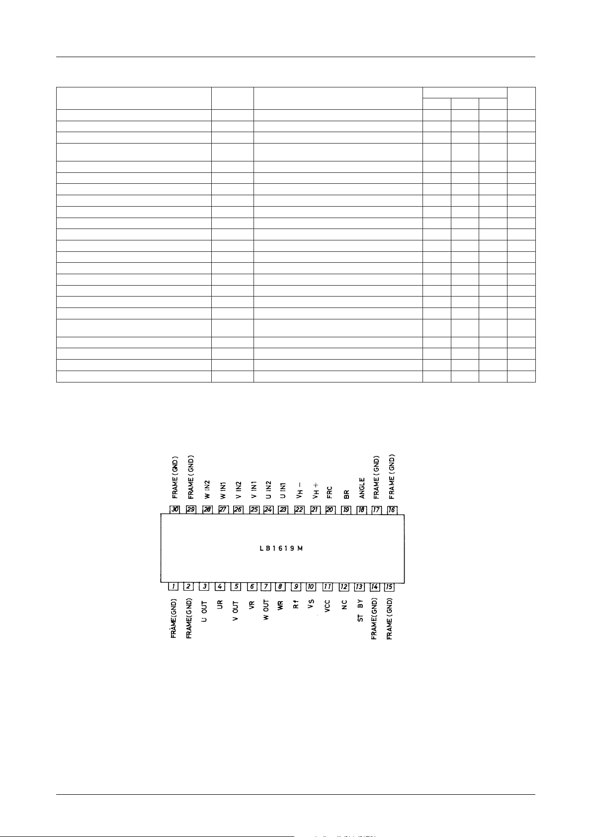
Pin Assignment
Note : All FRAME pins are connected to GND.
No.3323–2/7
Page 3
Truth Table
LB1619M
knisecruoS
1
2
3
4
5
6
esahpW → esahpV
esahpV → esahpWH
esahpW → esahpU
esahpU → esahpWH
esahpV → esahpW
esahpW → esahpVH
esahpU → esahpV
esahpV → esahpUH
esahpV → esahpU
esahpU → esahpVH
esahpU → esahpW
esahpW → esahpUH
tupnI
UVW
HHL
HLL
LLH
LHL
HLH
LHH
esreveR/drawroF
lortnoC
L
L
Input :
H : High level. One of the inputs should hav e a potential at least
0.2V higher than the other.
L : Low level. One of the inputs should ha ve a potential at least
0.2V lower than the other.
L
Forward/reverse control :
H : 2.8 to 5V
L : 0 to 1.2V
L
L
L
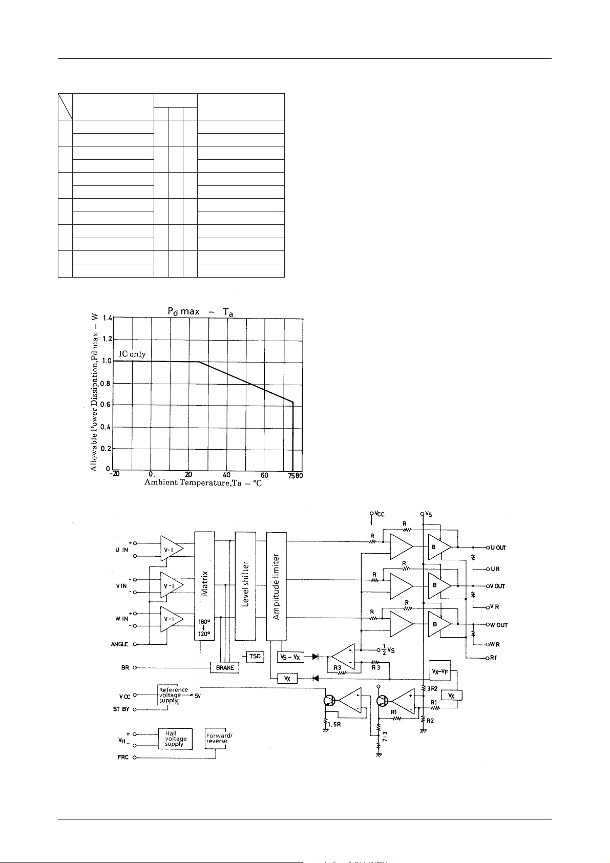
Equivalent Circuit Block Diagram
No.3323–3/7
Page 4

LB1619M
Pin Function Unit (resistance : Ω)
niP
.oN
2,1
51,41
71,61
03,92
3
5
7
niP
lobmyS
EMARF
DNG(
U
tuo
V
tuo
W
tuo
egatloVniPtiucriCtnelaviuqEnoitpircseDniP
.tuptuonahtrehtorofDNG
.sniptuptuO
4
6
8
9fR .rotsisnarttuptuorofDNG
01VSV<CC2 nahtrewolebtsuM.edutilpmatuptuoehtgnixifrofnipylppusrewoP
11V
31YB,TSxamV1.0:L
81ELGNA degnahcebnac)mrofevawrotomfoepols(niagtuptuo-tupnillahehT
U
R
RV
W
R
CC
nimV0.2:H
V
CC
≈ k01 Ω.
2forotsiserhtiwsniptuptuO Ω.
.egatlov2
revirdrotomnahtrehtotiucricreifilpmarewoprofnipylppusrewoP
.rotsisnart
sihtnI.gnitarepospotsyrtiucricehtlla,dednuorgsinipsihtnehW
lamronehtnI.Aµ001yletamixorppasitnerrucylppuseht,esac
folaitnetopataebotedamronepotfelsinipsiht,edomnoitarepo
.V2nahterom
.DNGdnanipsihtssorcadetcennocecnatsiserehtgnignahcyb
91RBnimV0.2:H
xamV8.0:L
rotomehtgnippotsrofniP
.)V8.0nahtsseL(evirdrotoM:levelL
.)V0.2nahteroM(potsrotoM:levelH
Continued on next page.
No.3323–4/7
Page 5

LB1619M
Continued from preceding page. Unit (resistance : Ω)
niP
.oN
02CRFnimV8.2:H
niP
lobmyS
egatloVniPtiucriCtnelaviuqEnoitpircseDniP
xamV2.1:L
.rotomfolortnocesrever/drawrofrofniP
.)V2.1nahtsseL(drawroF:levelL
.)V8.2nahteroM(esreveR:levelH
V
H
HV
UNI1
UNI2
VNI1
VNI2
WNI1
WNI2
+
–
nimV4.1
xamV8.2
12
22
32
42
52
62
72
82
Note) Pin 12 (NC pin) must be left open.
Sample Application Circuit
.tnerrucsaibllahehtgniylppusrofniP
.niptupnitnemelellahesahpU
U:"H"cigoL
U>1NI2
NI
V:"H"cigoL
V>1NI2
NI
W:"H"cigoL
W>1NI2
NI
.niptupnitnemelellahesahpV
.niptupnitnemelellahesahpW
+
V(ssorcadepolevedsiV1yletamixorppafoegatlovA
H
–
HV(dna)
.)
No.3323–5/7
Page 6

LB1619M
Output Voltage Waveform
Upper overlap=(2Vα–VA–VXL) / (VA–VXL)×100[%]
Lower overlap=(VA+VXL–2Vβ) / (VA–VXL)×100[%]
1. Upper overlap
DC voltage of upper amplitude : VS–VXH=V
DC voltage of lower amplitude : V
XL
Let the DC voltage at the intersection of two phases of the upper waveform be Vα :
From the drawing shown above
At upper overlap amount=A/B×100[%]
A =Vα–1/2(VS–VXH+VXL)=Vα–1/2(VA+VXL)
B =(VS–VXH)–1/2(VS–VXH+VXL)=1/2(VA+VXL)
* Upper overlap
=(2Vα–VA–VXL) / (VA–VXL)×100[%]
A
2. Lower overlap
DC voltage of upper amplitude : VS–VXH=V
DC voltage of lower amplitude : V
XL
A
Let the DC voltage at the intersection of two phases of the upper waveform be Vβ :
From the drawing shown above
At lower overlap amount=C/D×100[%]
C =1/2(VS–VXH+VXL)–Vβ=1/2(VA+VXL)–Vβ
D =1/2(VS–VXH+VXL)–VXL=1/2(VA–VXL)
* Lower overlap
=(VA–VXL–2Vβ) / (VA–VXL)×100[%]
No.3323–6/7
Page 7

LB1619M
Specifications of any and all SANYO products described or contained herein stipulate the performance,
characteristics, and functions of the described products in the independent state, and are not guarantees
of the performance, characteristics, and functions of the described products as mounted in the customer's
products or equipment. To verify symptoms and states that cannot be evaluated in an independent device,
the customer should always evaluate and test devices mounted in the customer's products or equipment.
SANYO Electric Co., Ltd. strives to supply high-quality high-reliability products. However, any and all
semiconductor products fail with some probability. It is possible that these probabilistic failures could
give rise to accidents or events that could endanger human lives, that could give rise to smoke or fire,
or that could cause damage to other property. When designing equipment, adopt safety measures so
that these kinds of accidents or events cannot occur. Such measures include but are not limited to protective
circuits and error prevention circuits for safe design, redundant design, and structural design.
In the event that any or all SANYO products(including technical data,services) described or
contained herein are controlled under any of applicable local export control laws and regulations,
such products must not be exported without obtaining the export license from the authorities
concerned in accordance with the above law.
No part of this publication may be reproduced or transmitted in any form or by any means, electronic or
mechanical, including photocopying and recording, or any information storage or retrieval system,
or otherwise, without the prior written permission of SANYO Electric Co. , Ltd.
Any and all information described or contained herein are subject to change without notice due to
product/technology improvement, etc. When designing equipment, refer to the "Delivery Specification"
for the SANYO product that you intend to use.
Information (including circuit diagrams and circuit parameters) herein is for example only ; it is not
guaranteed for volume production. SANYO believes information herein is accurate and reliable, but
no guarantees are made or implied regarding its use or any infringements of intellectual property rights
or other rights of third parties.
This catalog provides information as of February, 2001. Specifications and information herein are subject
to change without notice.
PS No.3323–7/7
 Loading...