

Ordering number : ENN*6181A
Preliminary
LB11996,11996H
Monolithic Digital IC
LB11996,11996H
Three-Phase Brushless Motor Driver
for CD-ROM Spindle Motor Driver
Features
• Current linear drive
• Control V type amplifier
• Separate power supply for output upper side bias
circuit allows low output saturation by boosting this
power supply only (useful for 5V power supply types).
• Upper side current detection technique loses loss
voltage of current detection resistor. Voltage drop
caused by this resistor reduces internal power
dissipation of IC.
• Built-in short braking circuit
• Built-in reverse blocking circuit
• Hall FG output
• Built-in S/S function
• Built-in current limiter circuit
• Built-in Hall power supply
• Built-in thermal shutdown circuit
• 1 Hall FG/3 Hall FG switchable
• Supports 3.3V DSP
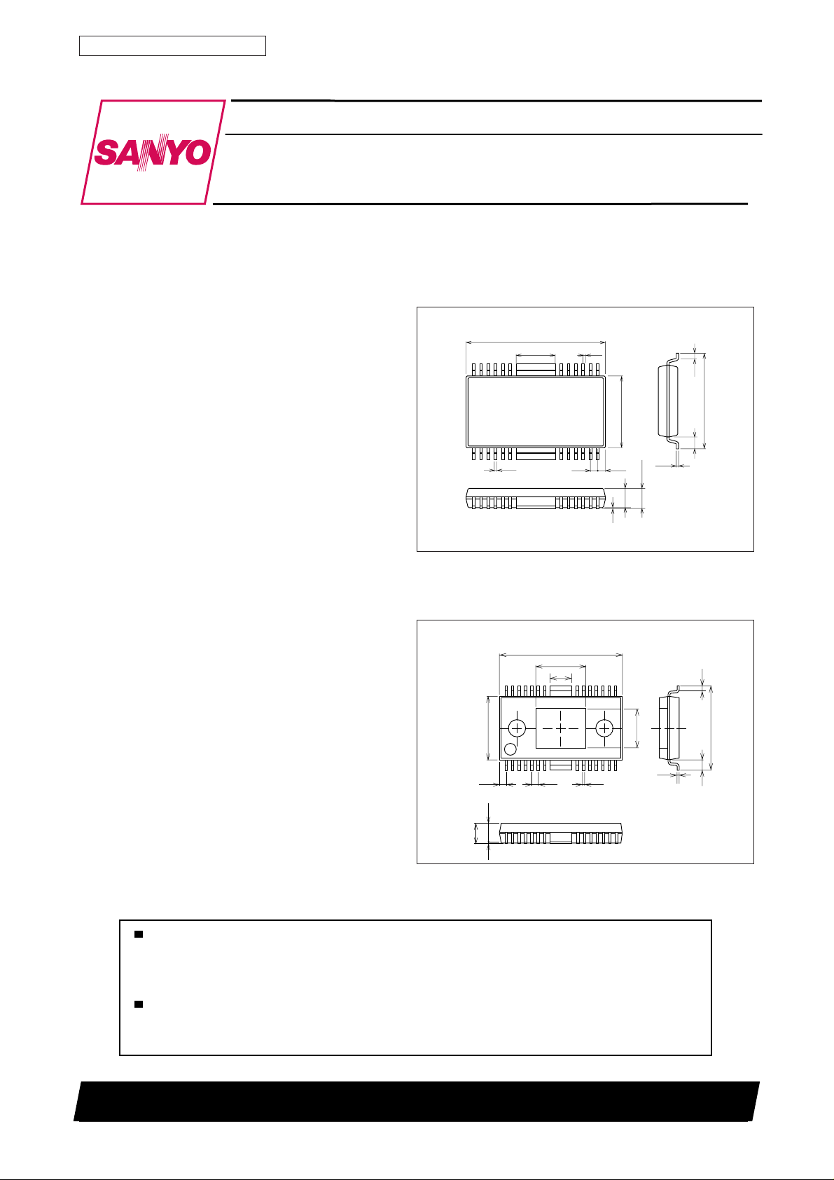
Package Dimensions
unit: mm
3227-HSOP24
[LB11996]
15.3
24
1
unit: mm
3234-HSOP28HC
4.3 0.3
0.3
0.8 0.85
[LB11996H]
15.3
6.2
28 15
2.7
13
7.9
12
2.25
0.1
0.65
10.5
1.3
0.25
2.5max
SANYO : HSOP24
0.65
7.9
1
0.85
2.25
2.5max
0.1
Any and all SANYO products described or contained herein do not have specifications that can handle
applications that require extremely high levels of reliability, such as life-support systems, aircraft's
control systems, or other applications whose failure can be reasonably expected to result in serious
physical and/or material damage. Consult with your SANYO representative nearest you before using
any SANYO products described or contained herein in such applications.
SANYO assumes no responsibility for equipment failures that result from using products at values that
exceed, even momentarily, rated values (such as maximum ratings, operating condition ranges, or other
parameters) listed in products specifications of any and all SANYO products described or contained
herein.
0.8
0.3
4.9
0.25
SANYO : HSOP28HC
SANYO Electric Co.,Ltd. Semiconductor Company
TOKYO OFFICE Tokyo Bldg., 1-10, 1 Chome, Ueno, T aito-ku, TOKYO, 110-8534 JAPAN
N0199RM(KI)
10.5
1.3
No. 6181-1/10
LB11996,11996H
Specifications
Absolute Maximum Ratings at Ta = 25°C
Parameter Symbol Conditions Ratings Unit
Maximum power supply voltage 1 7.0 V
Maximum power supply voltage 2 14.4 V
Maximum power supply voltage 3 14.4 V
Maximum applied output voltage Vo max 14.4 V
Maximum applied intput voltage Vi max V
Maximum output current Io max 1.3 A
Allowable power dissipation Pd max [LB11996] IC only 0.79 W
Operating temperature Topr –20 to +75 °C
Storage temperature Tstg –55 to +150 °C
* Specified substrate: 114.3 × 76.1 × 1.6 mm
Allowable Operating Ranges at Ta = 25°C
Parameter Symbol Conditions Ratings Unit
Power supply voltage 1 4 to 6 V
Power supply voltage 2 4 to 13.6 V
Power supply voltage 3 4 to 13.6 V
VCC1 max
VCC2 max
V
3 max
CC
3
glass epoxy
VCC1
VCC2
3
V
CC
V
CC
*With specified substrate *1.8
[LB11996H] IC only 0.8
*With specified substrate *1.9
1
≥V
CC
1
Sample Application at Ta = 25°C
(1) 12V type
Power supply pin Ratings Unit
V
CC
VCC1
2 = VCC3
Regulated voltage
Unregulated voltage
Conditions
(2) 5V type
Power supply pin Ratings Unit
VCC1 = VCC3
VCC2
Regulated voltage
Boost-up voltage or regulated voltage (Note)
Note: When boost-up voltage is used at VCC2, output can be set to low-saturation.
Conditions
4 to 6 V
4 to 13.6 V
4 to 6 V
4 to 13.6 V
No. 6181-2/10
LB11996,11996H
Electrical Characteristics at Ta = 25°C, VCC1 = 5V, VCC2 = VCC3 = 12V (unless otherwise specified)
Parameter Symbol
Conditions
[Power supply current]
V
Power supply current 1 8 mA
Power supply current 2 0 mA
Power supply current 3 150 250 µA
Output idle current 1 200 µA
Output idle current 2 30 µA
Output idle current 3 30 µA
VCC1
VCC2
V
I
CC
I
CC
I
CC
CC
1OQ
2OQ
3OQ
= V
C
CREF
VC = V
CREF
VC = V
3
CREF
V
= 0V
S/S
= 0V
V
S/S
V
= 0V
S/S
[Output]
V
1
Saturation voltage, upper side 1 V
Saturation voltage, lower side 1 0.3 V
Saturation voltage, upper side 2 0.3 V
Saturation voltage, lower side 2 0.3 V
Current limiter setting voltage 0.37 V
VOD1
V
V
V
IO = –0.5A, VCC1 = 5V, VCC2 = VCC3 = 12V
OU
IO = 0.5A, VCC1 = 5V, VCC2 = VCC3 = 12V
2
I
OU
OD
CL
= –0.5A, VCC1 = VCC3 = 5V, VCC2 = 12V
O
2
= 0.5A, VCC1 = VCC3 = 5V, VCC2 = 12V
I
O
RRF = 0.33Ω
[Hall amplifier]
Common mode input voltage range 1.2 V
Input bias current 1 µA
Minimum Hall input level 60 mVp-p
V
HCOM
V
V
HIB
HIN
[S/S pin]
High level voltage 2.0 V
Low level voltage 0.7 V
Input current 200 µA
Leakage current –30 µA
V
V
I
I
S/SH
S/SL
S/SI
S/SL
V
= 5V
S/S
V
= 0V
S/S
[Control]
VC pin input current 1 µA
VCREF pin input current 1 µA
Voltage gain 0.35 times
Startup voltage 1.5 1.8 V
Startup voltage width 50 150 mV
I
IV
GV
V
∆V
VC
CREF
CC
CTH
CTH
VC = V
VC = V
∆V
RF
V
CREF
V
CREF
CREF
CREF
/∆V
C
= 1.65V
= 1.65V
= 1.65V
= 1.65V
[Hall power supply]
Hall power supply voltage 0.8 V
Allowable current 20 mA
V
H
I
H
= 5 mA
I
H
[Thermal shutdown]
Operating temperature (Target) 150 180 210 °C
Hysteresis (Target) 15 °C
T
∆T
TSD
TSD
[Short braking]
Brake pin at High level 45V
Brake pin at Low level 01V
V
BRH
V
BRL
[1 Hall FG/3 Hall FG select]
FGSEL pin at High level 45V
FGSEL pin at Low level 01V
V
FSH
V
FSL
Note:
• During S/S OFF (standby), the Hall comparator is at High.
• Items shown to be “Target” are not measured.
Ratings
min typ max
1.0
V
1–1.0
CC
V
CC
Unit
1
No. 6181-3/10
 Loading...