SANYO LB11985H Datasheet

Ordering number :ENN6209B
12800RM (OT) No. 6209-1/9
Functions
• Three-phase current linear drive with switching between
full-wave and half-wave operations
• Torque ripple correction circuit
• Current limiter circuit
• Upper and lower sides output stage saturation prevention
circuits
• Short brake circuit
• FG amplifier
• Thermal shutdown circuit
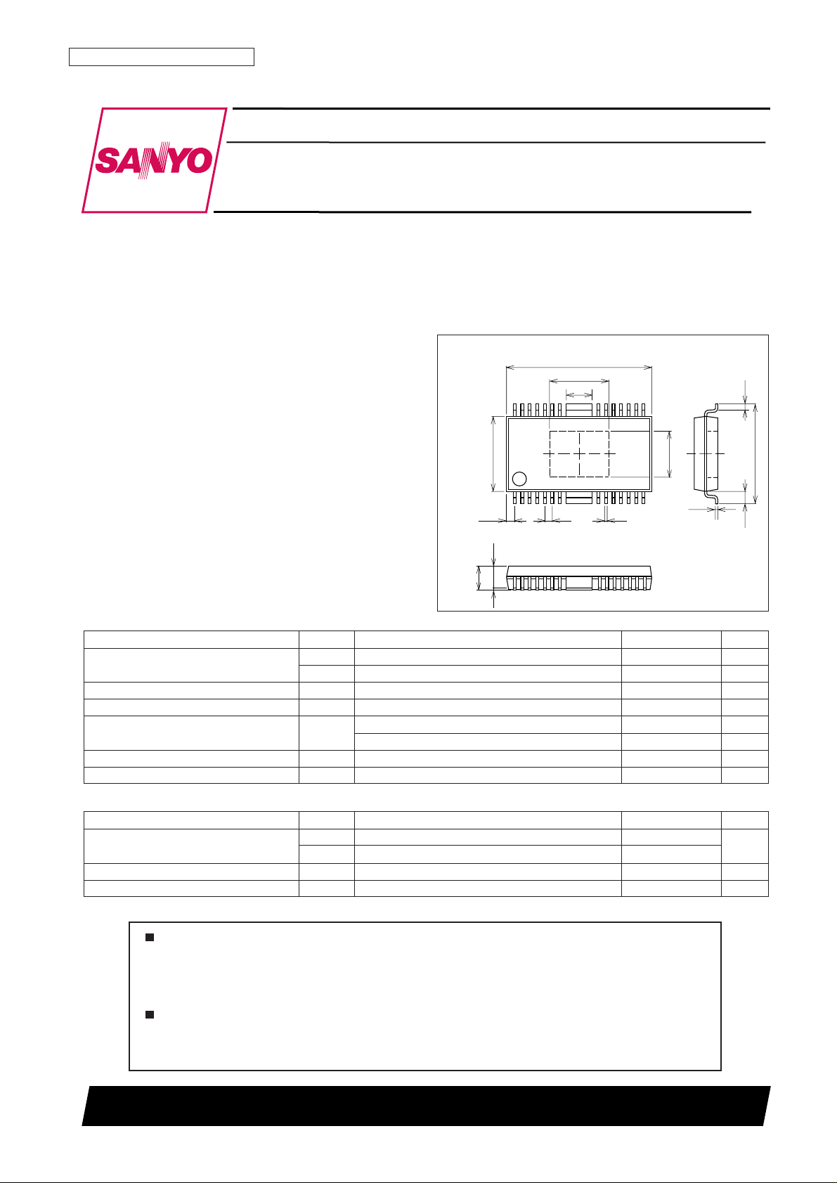
Package Dimensions
unit: mm
3233-HSOP28H
6.2
28 15
114
0.8
15.3
2.7
0.3
4.9
1.3
10.5
0.65
0.25
0.85
7.9
2.25
2.5max
0.1
SANYO: HSOP28H
[LB11985H]
SANYO Electric Co.,Ltd. Semiconductor Company
TOKYO OFFICE Tokyo Bldg., 1-10, 1 Chome, Ueno, Taito-ku, TOKYO, 110-8534 JAPAN
Monolithic Digital IC
LB11985H
VCR Capstan Motor Brushless Motor Driver
Any and all SANYO products described or contained herein do not have specifications that can handle
applications that require extremely high levels of reliability, such as life-support systems, aircraft’s
control systems, or other applications whose failure can be reasonably expected to result in serious
physical and/or material damage. Consult with your SANYO representative nearest you before using
any SANYO products described or contained herein in such applications.
SANYO assumes no responsibility for equipment failures that result from using products at values that
exceed, even momentarily, rated values (such as maximum ratings, operating condition ranges, or other
parameters) listed in products specifications of any and all SANYO products described or contained
herein.
Parameter Symbol Conditions Ratings Unit
Maximum supply voltage
V
CC
max 6V
V
S
max 15.5 V
Maximum output current I
O
max 1.5 A
Maximum output voltage V
O
max 30 V
Allowable power dissipation Pdmax
Independent IC 0.8 W
76.1
× 114.3 × 1.6 mm3: With glass epoxy 2.0 W
Operating temperature Topr –20 to +75 °C
Storage temperature Tstg –55 to +150 °C
Specifications
Absolute Maximum Ratings at Ta = 25°C
Parameter Symbol Conditions Ratings Unit
Supply voltage
V
S
8 to 15
V
V
CC
4.5 to 5.5
Hall input amplitude V
HALL
Between Hall inputs ±20 to ±100 mV 0-P
GSENSE input range V
GSENSE
With respect to the control system ground –0.20 to +0.20 V
Allowable Operating Ranges at Ta = 25°C
Note : Forward/reverse switching is not possible in half-wave operation mode.

No. 6209-2/9
LB11985H
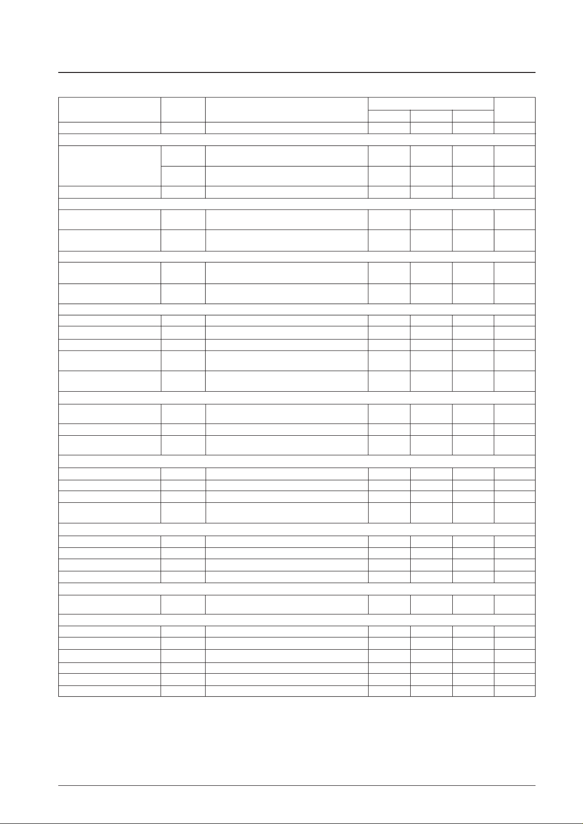
Electrical Characteristics at Ta = 25°C, VCC= 5 V, VS= 15 V
Parameter Symbol Conditions
Ratings
Unit
min typ max
V
CC
current drain I
CC
RL = ∞, VCTL = 0 V (quiescent mode) 10 15 mA
[Output]
Output saturation voltage
V
Osat
1
I
O
= 500 mA, Rf = 0.5 Ω, Sink + Source
2.2 2.7 V
VCTL = VLIM = 5 V (with saturation prevention)
V
Osat
2
I
O
= 1.0 A, Rf = 0.5 Ω, Sink + Source
2.8 3.7 V
VCTL = VLIM = 5 V (with saturation prevention)
Output leakage current I
Oleak
1.0 mA
[FR]
FR pin input
V
FR
14V
Threshold voltage
FR pin input
Ib (FR) VFR = 5 V 100 150 µA
Input bias current
[BR]
BR pin input
V
BRTH
14V
Threshold voltage
BR pin input
Ib (BR) VBR = 5 V 100 150 µA
Input bias current
[Control]
CTLREF pin voltage V
CREF
2.0 2.15 2.3 V
CTLREF pin input range V
CREF
IN 1 4 V
CTL pin input bias current Ib (CTL) VCTL = 5 V, with CTLREF open 5 µA
CTL pin control start voltage V
CTL
(ST)
Rf = 0.5 Ω, VLIM = 5 V, Io ≥ 40 mA
2.0 2.2 2.4 V
With the Hall input logic states fixed (U, V, W = high, high, low)
CTL pin control Gm Gm (CTL)
Rf = 0.5 Ω, ∆Io = 200 mA
1.8 2.25 2.7 V
With the Hall input logic states fixed (U, V, W = high, high, low)
[Current Limiter]
LIM current limit offset voltage V
off
(LIM)
Rf = 0.5 Ω, VCTL = 5 V, Io ≥ 40 mA
80 200 320 mV
With the Hall input logic states fixed (U, V, W = high, high, low)
LIM pin input bias current Ib (LIM) VCTL = 5 V,VREF: OPEN, VLIM = 0 V –2 –1 µA
LIM pin current limit level Gm (LIM)
Rf = 0.5 Ω, VCTL = 5 V
0.37 0.47 0.57 mA
With the Hall input logic states fixed (U, V, W = high, high, low)
[Hall Amplifier]
Input offset voltage V
off
(HALL) –6 +6 mV
Input bias current I
b
(HALL) 1.0 3.0 µA
Common-mode input voltage V
cm
(HALL) 1.3 3.3 V
Torque ripple correction ratio TRC
At the bottom and peak that occur in the Rf
14.5 %
waveform at 200 mA (Rf = 0.5 Ω)
[FG Amplifier]
FG amplifier input offset voltage
V
off
(FG) –8 +8 mV
FG amplifier input bias current I
b
(FG) –100 nA
FG amplifier output saturation voltage
V
Osat
(FG) For the sink side, at the internal pull-up resistor 0.4 0.55 V
FG amplifier common-mode input voltage
V
CM
(FG) 1.0 4.0 V
[Saturation]
Saturation prevention circuit V
Osat
(DET) Io = 10 mA, Rf = 0.5 Ω, VCTL = VLIM = 5 V
0.13 0.25 0.42 V
lower side set voltage
The voltages between the OUT-Rf pairs at full wave.
[Schmitt Amplifier]
Duty DUTY 60 mVp-p, 1 kHz input *
1
49 50 51 %
Upper side output saturation voltage
V
satu
(SH) 4.8 V
Lower side output saturation voltage
V
satd
(SH) 0.2 V
Hysteresis Vhys Design target values *
2
45 mV
TSD operating temperature T-TSD Design target values *
2
180 °C
TSD hysteresis ∆T-TSD Design target values *
2
15 °C
Note *1 : The ratings are just the measured value with no margin afforded.
*2 : Items shown to be design target values in the conditions column are not measured.

No. 6209-3/9
LB11985H
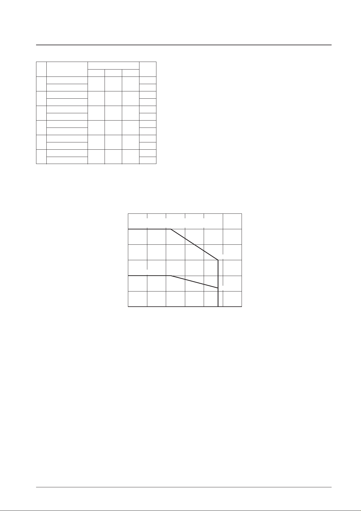
Truth Table and Control Functions
Source → Sink
Hall input
FR
UVW
1
V → W
HHL
H
W → VL
2
U → W
HLL
H
W → UL
3
U → V
HLH
H
V → UL
4
W → V
LLH
H
V → WL
5
W → U
LHH
H
U → WL
6
V → U
LHL
H
U → VL
Note: 1. In the FR column, “H” indicates a voltage of 2.75 V or higher, and “L”
indicates a voltage of 2.25 V or lower. (When V
CC
is 5 V.)
2. For the Hall inputs, the input high state is defined to be the state where
the (+) input is higher than the corresponding (–) input by at least 0.02 V,
and the input low state is defined to be the state where the (+) input is
lower than the corresponding (–) input by at least 0.02 V.
Allowable Power Dissipation
0.4
0
0.8
1.2
1.6
2.0
2.4
–20 0 20 40 60 80 100
Pd max — Ta
0.48
1.20
Allowable power dissipation, Pd [W]
Ambient temperature, Ta [°C]
Independent IC
Mounted on the specified printed circuit board
(76.1 × 114.3 × 1.6 mm3glass epoxy board)
 Loading...