

Ordering number : ENN6497A
11201RM (OT) No. 6497-1/12
Overview
The LB11975 is a monolithic bipolar IC developed for
uses as a spindle motor driver for high-speed CD-ROM
and DVD-ROM drives. To minimize heat generation
during high-speed rotation and braking, the LB11975
adopts direct PWM drive in the output stage. During
reverse braking the upper and lower side output transistors
are both driven in PWM mode to implement dual PWM
controlled braking. The device thus controls the current to
remain under a limit value and prevent rapid heat
generation. This prevents device destruction due to rapid
heating. The absolute maximum voltage rating is 27 V,
and the maximum current is 2.5 A.
Functions and Features
• Direct PWM drive (lower side control)
• Built-in upper and lower side output diodes
• Supports the use 3.3 V DSP devices.
• Power saving function for standby mode
• Hall FG output (1 or 3 Hall device operation)
• Built-in Hall device power supply
• Reverse rotation detection output and drive cutoff circuit
• Voltage control amplifier
• Current limiter circuit
• Thermal protection circuit
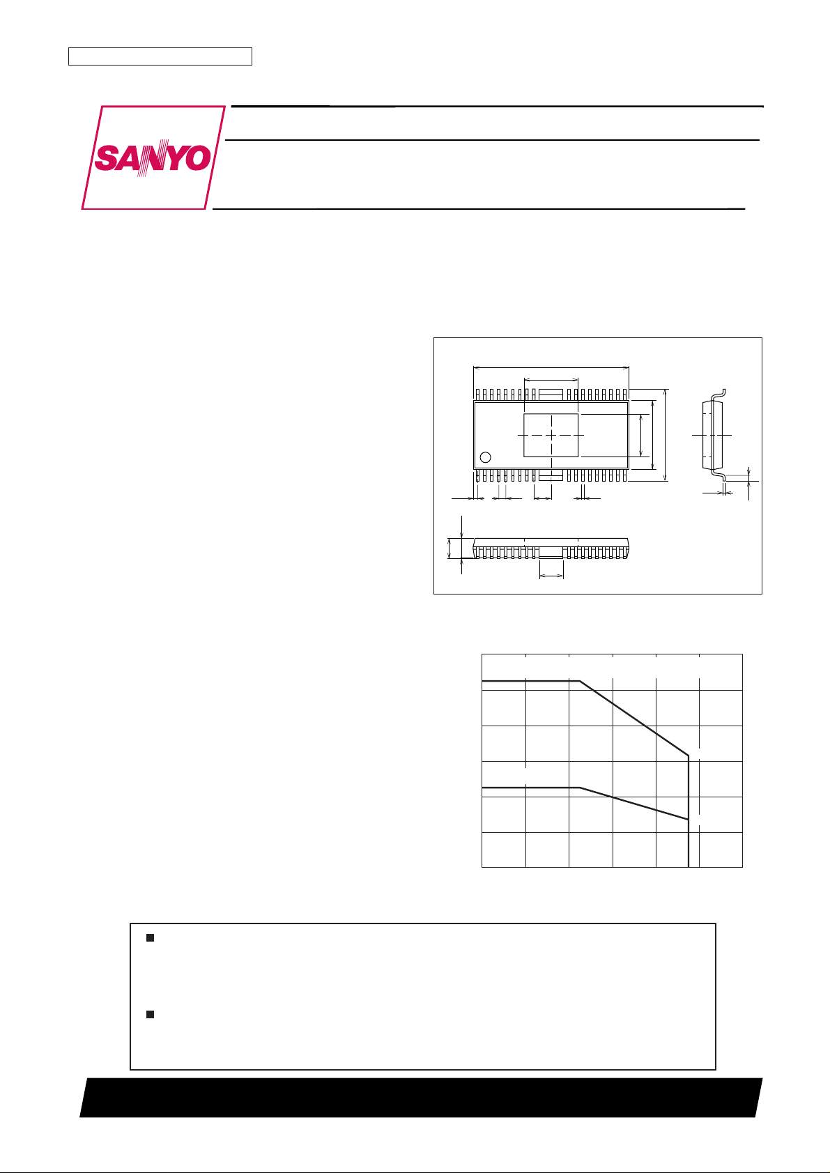
Package Dimensions
unit: mm
3251-HSOP36R
(6.2)
36
1
19
18
0.8
2.0
17.8
0.3
(4.9)
2.7
0.65
0.25
(0.5)
7.9
10.5
2.25
2.45max
0.1
SANYO: HSOP36R
[LB11975]
LB11975
SANYO Electric Co.,Ltd. Semiconductor Company
TOKYO OFFICE Tokyo Bldg., 1-10, 1 Chome, Ueno, Taito-ku, TOKYO, 110-8534 JAPAN
High-Speed CD-ROM Spindle Motor Driver IC
Monolithic Digital IC
Any and all SANYO products described or contained herein do not have specifications that can handle
applications that require extremely high levels of reliability, such as life-support systems, aircraft’s
control systems, or other applications whose failure can be reasonably expected to result in serious
physical and/or material damage. Consult with your SANYO representative nearest you before using
any SANYO products described or contained herein in such applications.
SANYO assumes no responsibility for equipment failures that result from using products at values that
exceed, even momentarily, rated values (such as maximum ratings, operating condition ranges, or other
parameters) listed in products specifications of any and all SANYO products described or contained
herein.
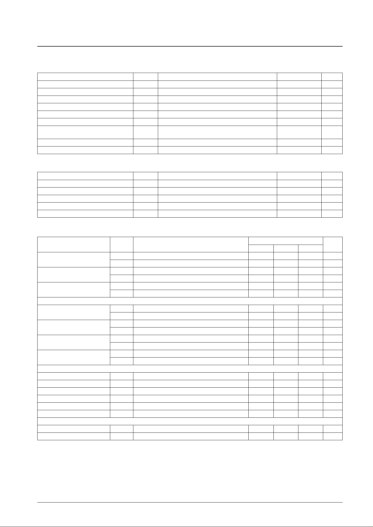
0.4
0
0.8
0.9
1.2
1.6
2.0
2.1
2.4
–20 0 20 40 60 80 100
Allowable power dissipation, Pd max — W
Pd max — Ta
Ambient temperature, Ta — °C
Mounted on the specified printed circuit
(114.3 × 76.1 × 1.6 mm3 glass epoxy board)
Independent IC
0.54
1.26
No. 6497-2/12
LB11975
Parameter Symbol Conditions Ratings Unit
Supply voltage 1 V
CC
1 max 7V
Supply voltage 2 V
CC
2 max 27 V
Supply voltage 3 V
CC
3 max 27 V
Output current I
O
max 2.5 A
Output applied voltage V
IN
max 30 V
Allowable power dissipation 1 Pd max1 Independent IC 0.9 W
Allowable power dissipation 2 Pd max2
Mounted on the specified circuit board
2.1 W
(114.3 × 76.1 × 1.6 mm
3
glass epoxy board)
Operating temperature Topr –20 to +75 °C
Storage temperature Tstg –55 to +150 °C
Specifications
Maximum Ratings at Ta = 25°C
Parameter Symbol Conditions Ratings Unit
Power-supply voltage range 1 V
CC
1 4 to 6 V
Power-supply voltage range 2 V
CC
2VCC2 ≥ VCC1 4 to 16 V
Power-supply voltage range 3 V
CC
3 4 to 16 V
FG pin applied voltage VFG 0 to V
CC
1V
FG pin output current IFG 0 to 4.0 mA
Allowable Operating Ranges at Ta = 25°C
Parameter Symbol Conditions
Ratings
Unit
min typ max
Supply current 1
I
CC
1-1 V
CTL
= V
CREF
5.0 8.0 11.0 mA
I
CC
1-2 VS/S = 0 V 0 200 µA
Supply current 2
I
CC
2-1 V
CTL
= V
CREF
5.0 6.5 8.0 mA
I
CC
2-2 VS/S = 0 V 0 200 µA
Supply current 3
I
CC
3-1 V
CTL
= V
CREF
0.3 0.7 mA
I
CC
3-2 VS/S = 0 V 0 200 µA
[Output Block]
Output saturation voltage 1
V
O
sat1(L) IO= 0.5 A, VO(sink), VCC1 = 5 V, VCC2 = VCC3 = 12 V 0.15 0.25 V
V
O
sat1(H) IO= 0.5 A, VO(source), VCC1 = 5 V, VCC2 = VCC3 = 12 V 0.80 0.95 V
Output saturation voltage 2
V
O
sat2(L) IO= 1.5 A, VO(sink), VCC1 = 5 V, VCC2 = VCC3 = 12 V 0.40 0.60 V
V
O
sat2(H) IO= 1.5 A, VO(source), VCC1 = 5 V, VCC2 = VCC3 = 12 V 1.10 1.30 V
Output leakage current
I
O
leak(L) 100 µA
I
O
leak(H) –100 µA
Diode forward voltage
V
F
H Upper side diode, IO= 2.0 A 1.50 2.00 V
V
F
L Lower side diode, IO= 2.0 A 1.50 2.00 V
[Hall Amplifier Block]
Input bias current I
HB
–4 –1 µA
Common-mode input voltage range
V
ICM
1.5
VCC– 1.5
V
Hall input sensitivity V
HIN
60 mVp-p
Hysteresis ∆V
IN
(HA) 23 32 39 mV
Input voltage: low → high V
SL
H 6 16 25 mV
Input voltage: high → low V
SL
L –25 –16 –6 mV
[Thermal Protection Circuit]
Operating temperature T-TSD Design target value (junction temperature) * 150 180 210 °C
Hysteresis ∆TSD Design target value (junction temperature) * 40 °C
Electrical Characteristics at Ta = 25°C, VCC1 = 5 V, VCC2 = VS= 12 V
Continued on next page.
Note: * These are design target values and are not tested.
No. 6497-3/12
LB11975
Continued from preceding page.
Parameter Symbol Conditions
Ratings
Unit
min typ max
[PWM Oscillator]
High-level output voltage V
O
H(OSC) 3.1 3.3 3.5 V
Low-level output voltage V
O
L(OSC) 1.4 1.6 1.8 V
Amplitude V(OSC) 1.5 1.7 1.9 Vp-p
Oscillator frequency f(OSC) C = 2200 pF 23.0 kHz
Charge current I
CHG
–110 –94 –83 µA
Charge resistor value R
DCHG
1.6 2.1 2.6 kΩ
[CTL Amplifier]
VCTL pin input current I
VCTLVCTL
= V
CREF
= 1.65 V –2 µA
VCREF pin input current I
VCREFVCTL
= V
CREF
= 1.65 V –2 µA
Forward rotation gain GDF
+
Design target value * 0.20 0.25 0.30 times
Reverse rotation gain GDF
–
Design target value * –0.30 –0.25 –0.20 times
Forward rotation limiter voltage V
RF
1 0.26 0.29 0.32 V
Reverse rotation limiter voltage V
RF
2 0.26 0.29 0.32 V
Startup voltage V
CTHVCREF
= 1.65 V. Design target value * 1.50 1.80 V
Dead zone V
DZVCREF
= 1.65 V. Design target value * 35 80 140 mV
[FG Pin] (speed pulse output)
Low-level output voltage V
FGLIFG
= 2 mA 0.4 V
Pull-up resistor value R
FG
7.5 10 12.5 kΩ
[RS Pin]
Low-level output voltage V
RSLIRS
= 2 mA 0.4 V
Pull-up resistor value R
RS
7.5 10 12.5 kΩ
[Stop/Start Pin]
Low-level input voltage V
SS
L 0 0.7 V
High-level input voltage V
SS
H 2.0 VCC1V
Low-level input current I
SS
LVSS= 0 V –1 0 µA
High-level input current I
SS
HVSS= 5.0 V 50 200 µA
[Hall Device Power Supply]
Hall device supply voltage V
HIH
= 5 mA 0.65 0.85 1.05 V
Allowable current I
H
20 mA
Truth Table
Input Control voltage V
CTL
Output FG output
IN1 IN2 IN3 Source → Sink FG1 FG2
1HLH
H OUT2 → OUT1
LH
L OUT1 → OUT2
2HLL
H OUT3 → OUT1
LL
L OUT1 → OUT3
3HHL
H OUT3 → OUT2
LH
L OUT2 → OUT3
4LHL
H OUT1 → OUT2
HL
L OUT2 → OUT1
5LHH
H OUT1 → OUT3
HH
L OUT3 → OUT1
6LLH
H OUT2 → OUT3
HL
L OUT3 → OUT2
Note: * These are design target values and are not tested.
FG1
FG2
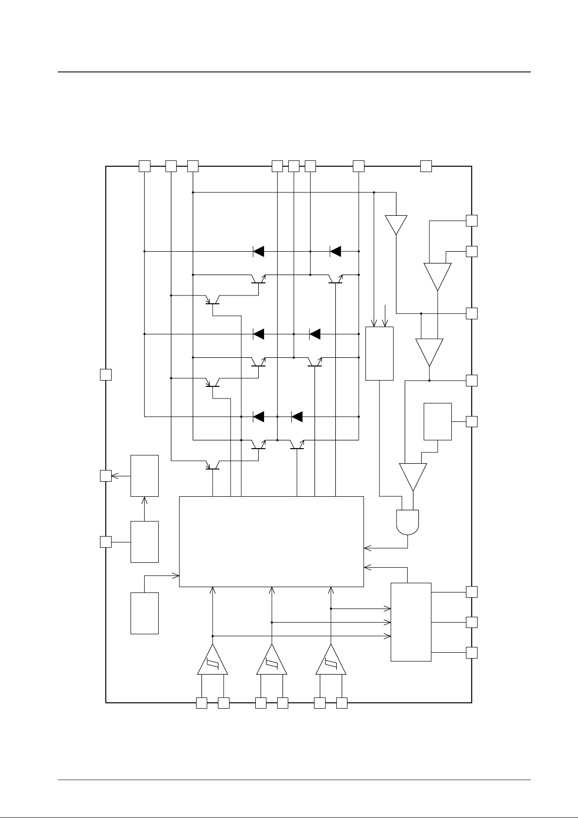
Block Diagram
No. 6497-4/12
LB11975
23
IN1
+
IN1
–
IN2
–
IN3
–
IN2
+
IN3
+
28
9
15
22
21
20
19
18
MATRIX
&
LOGIC
TSD
V
CC
3
OSC
Rotation direction
detection
S/S
16 27
HALL
BIAS
CURR
LIM
141312
PH
1110
PWM FC V
CREF
V
CTL
GND1
(7, 30, 31)
GND2
(4)
OUT3
(2)
OUT2
(36)
OUT1
Rf
V
CC
2
(29)
V
CC
3
V
CC
1
VHS/S
25
FG2
26
FG1
24
RS
A13185
8
35
1
3
6
17
 Loading...