

Ordering number : ENN6470
52600RM (OT) No. 6470-1/9
Overview
The LB11880 is a sensorless motor driver that also
includes a loading motor driver. It is ideal for drum motor
drive in VCR products.
Functions and Features
• Soft switching drive
• No Hall sensors required
• No FG sensors required
• Built-in PG amplifier
• Built-in thermal shutdown circuit
• Current limiter circuit
• On-chip loading motor driver
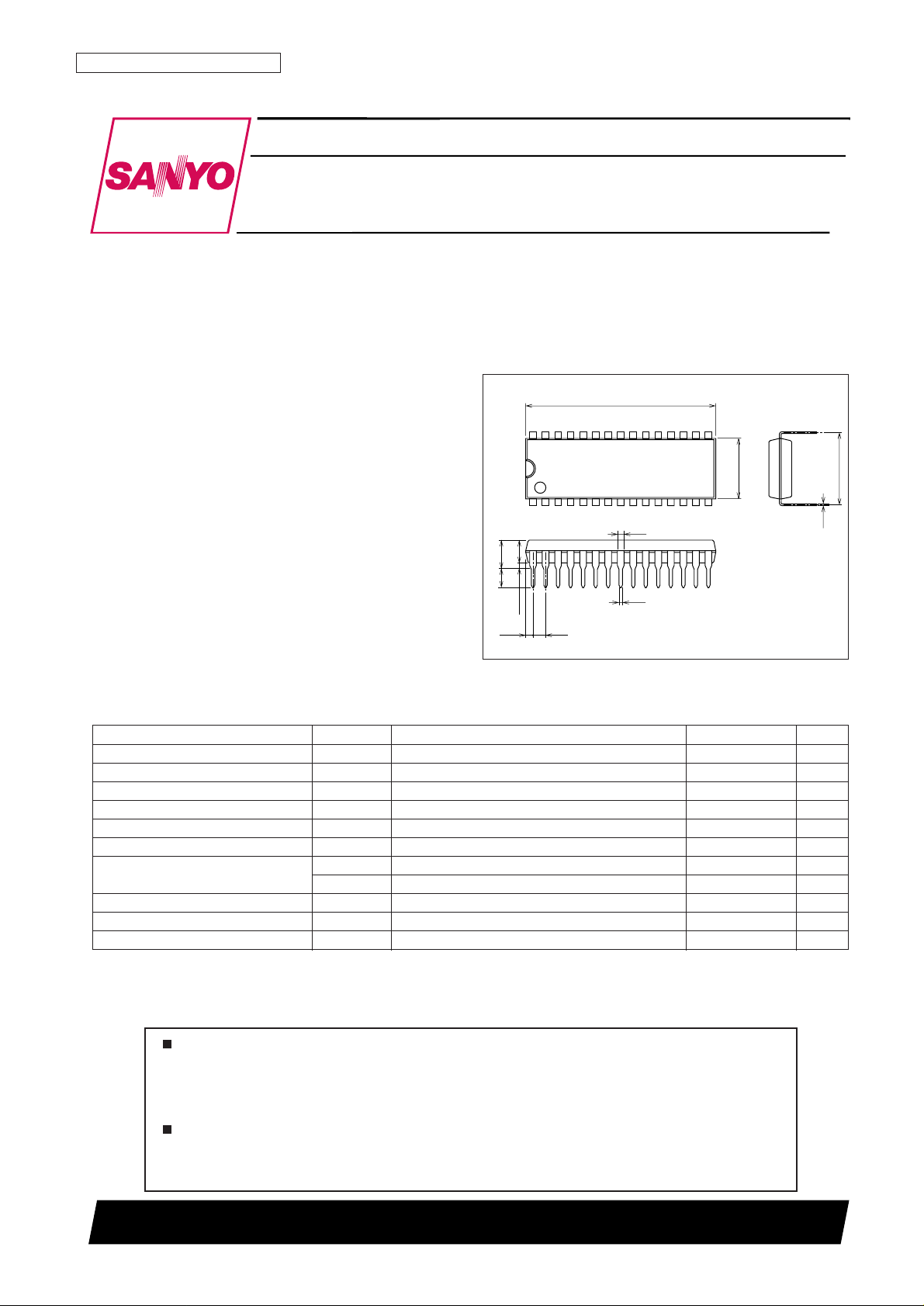
Package Dimensions
unit: mm
3196A-DIP30SD
(1.04)
1.78
0.95
0.48
10.16
3.95mas
(3.25)
0.51min
3.0
0.25
115
30 16
8.6
27.0
SANYO: DIP30SD
[LB11880]
LB11880
SANYO Electric Co.,Ltd. Semiconductor Company
TOKYO OFFICE Tokyo Bldg., 1-10, 1 Chome, Ueno, Taito-ku, TOKYO, 110-8534 JAPAN
Three-Phase Sensorless Motor Driver with
Loading Motor Driver
Monolithic Digital IC
Any and all SANYO products described or contained herein do not have specifications that can handle
applications that require extremely high levels of reliability, such as life-support systems, aircraft’s
control systems, or other applications whose failure can be reasonably expected to result in serious
physical and/or material damage. Consult with your SANYO representative nearest you before using
any SANYO products described or contained herein in such applications.
SANYO assumes no responsibility for equipment failures that result from using products at values that
exceed, even momentarily, rated values (such as maximum ratings, operating condition ranges, or other
parameters) listed in products specifications of any and all SANYO products described or contained
herein.
Parameter Symbol Conditions Ratings Unit
Maximum supply voltage 1 V
CC
max 14.5 V
Maximum supply voltage 2 V
CC
L max 14.5 V
Maximum supply voltage 3 VREG max 7.0 V
Output voltage Vomax 14.5 V
Input voltage VI1max –0.3 to VREG + 0.3 V
Cylinder current Iomax 1.0 A
Loading current
Iomax (AVE) 0.4 A
Iomax (peak) 1.2 A
Allowable power dissipation Pdmax When mounted on the specified printed circuit board* 2.8 W
Operating temperature Topr –20 to +75 °C
Storage temperature Tstg –55 to +150 °C
Specifications
Absolute Maximum Ratings at Ta = 25°C
Note: * Specified printed circuit board: 114.3 × 76.1 × 1.6 mm glass-epoxy board
No. 6470-2/9
LB11880
Parameter Symbol Conditions Ratings Unit
Supply voltage 1 V
CC
8 to 13.8 V
Supply voltage 2 V
CC
L 8 to 13.8 V
Supply voltage 3 VREG 4 to 6 V
Allowable Operating Ranges at Ta = 25°C
Parameter Symbol Conditions
Ratings
Unit
min typ max
Supply current 1 I
CC
VC = 0 V, XIN = YIN = 0 V 3.5 5.0 mA
Supply current 2 I
CC
L VC = 0 V, XIN = YIN = 0 V 1 mA
Supply current 3 I
REG
VC = 0 V, XIN = YIN = 0 V 10 15 mA
Output saturation voltage 1 V
O
sat1 IO = 0.4 A, source + sink 1.4 2.0 V
Output saturation voltage 2 V
O
sat2 IO = 0.8 A, source + sink 1.8 2.6 V
MC pin common-mode input voltage range V
IC
0V
CC
– 2 V
VC pin input bias current I
VC
VC = 0 V –2 –1 µA
Control start voltage VTHVC VRF = 10 mA 2.4 2.5 2.6 V
Closed-loop control gain GMVC RF = 0.5 Ω 0.75 0.95 1.15 A/V
PCOUT output current 1 I
PCO
U Source side –90 µA
PCOUT output current 2 I
PCO
D Sink side 90 µA
VCOIN input current I
VCO
IN VCOIN = 5 V 0.1 0.2 µA
Minimum VCO frequency f
VCO
MIN CX = 0.022 µF, VCOIN = open 400 Hz
Maximum VCO frequency f
VCO
MAX CX = 0.022 µF, VCOIN = 5 V 18.5 kHz
C1/C2 source current ratio R
SOURCEIC1SOURCE/IC2SOURCE
–12 +12 %
C1/C2 sink current ratio R
SINKIC1SINK/IC2SINK
–12 +12 %
C1 source/sink current ratio RC1 I
C1SOURCE/IC1SINK
–35 +15 %
C2 source/sink current ratio RC2 I
C2SOURCE/IC2SINK
–35 +15 %
Thermal shutdown operating temperature T-TSD * 150 180 210 °C
Thermal shutdown hysteresis ∆TTSD * 15 °C
Electrical Characteristics at Ta = 25°C, VCC= VCCL = 12 V, VREG = 5 V
Parameter Symbol Conditions
Ratings
Unit
min typ max
[Back EMF FG]
Output on voltage V
O
L 0.4 V
Output off voltage V
O
H 4.5 V
[PG Amplifier]
Input offset voltage V
I
O–8+8mV
Input bias current I
B
IN– –250 nA
Common-mode input voltage range V
ICOM
* 1 3.5 V
Open-loop gain GVPG f = 1 kHz 55 dB
Output on voltage V
O
L 0.4 V
Output off voltage V
O
H 4.5 V
Schmitt amplifier hysteresis V
S
hys 70 93 115 mV
FG/PG Amplifier Block at Ta = 25°C, VCC= VCCL = 12 V, VREG = 5 V
Note: * These values are design guarantee values, and are not tested.
Note: * These values are design guarantee values, and are not tested.
No. 6470-3/9
LB11880
Parameter Symbol Conditions
Ratings
Unit
min typ max
Input voltage
1 (high) V
IN
1 3.5 5 V
2 (low) V
IN
2 0 0.8 V
Input current I
IN
Sink VIN= 3.5 V 30 50 µA
Input hysteresis ∆VT 0.7 V
Vsat U-1
Vref = VS, between the output and VS
1.5 2.1 V
I
O
= 0.2 A, CW/CCW mode
Vsat L-1
Vref = VS, between the output and ground
0.2 0.3 V
Saturation voltage
I
O
= 0.2 A, CW/CCW mode
Vsat U-1’
Vref = VS, between the output and VS
1.6 2.2 V
IO= 0.4 A, CW/CCW mode
Vsat L-1’
Vref = VS, between the output and ground
0.3 0.5 V
IO= 0.4 A, CW/CCW mode
VsatU-1’’
Vref = 8 V, between the output and ground
7.2 8.0 8.8 V
Upper side residual voltage
I
O
= 0.2 A, CW/CCW mode
VsatL-1’’
Vref = 8 V, between the output and ground
7.2 8.0 8.8 V
IO= 0.4 A, CW/CCW mode
Output transistor leakage current
Upper ILU 50 µA
Lower ILL 50 µA
Diode forward voltage
Uper VFU IF = 0.4 A 1.3 V
Lower VFL IF = 0.4 A 1.0 V
Control supply current Iref –5 –2 µA
Loading Block at Ta = 25°C, VCC= VCCL = 12 V, VREG = 5 V
 Loading...