SANYO LB11824M Datasheet
Ordering number : ENN7107
80102RM (OT) No. 7107-1/17
Overview
The LB11824M is a direct PWM drive predriver IC for
use with three-phase power brushless motors. The
LB11824M can implement a motor drive circuit with the
desired output capacity (voltage and current) by using
appropriate external transistors. This device is optimal for
motor drive in larger home appliances such as air
conditioners and on-demand hot water heaters.
Functions and Features
• Three-phase bipolar drive
• Direct PWM drive
• Built-in forward/reverse switching circuit
• Full complement of built-in protection circuits,
including current limiter, undervoltage protection
circuit, motor lockup protection circuit, and thermal
protection circuit.
• Can be controlled by either a command voltage or the
duty of an input PWM signal.
• Provides three types of Hall-effect element signal pulse
outputs.
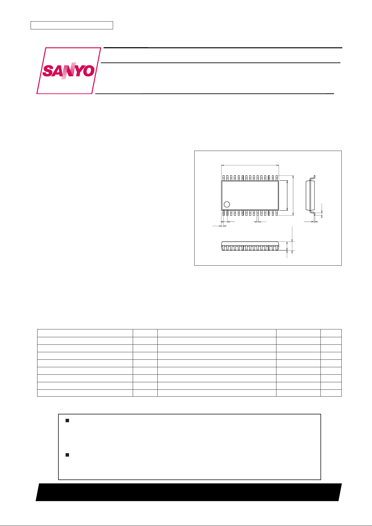
Package Dimensions
unit: mm
3073C-MFP30SD
1
15
30 16
1.0
15.2
0.4
0.65
10.5
7.9
0.25
(0.6)
2.45max
0.1
(2.25)
SANYO: MFP30SD
[LB11824M]
LB11824M
SANYO Electric Co.,Ltd. Semiconductor Company
TOKYO OFFICE Tokyo Bldg., 1-10, 1 Chome, Ueno, Taito-ku, TOKYO, 110-8534 JAPAN
Direct PWM Drive Brushless Motor Predriver for On-Demand Water Heater
and Air Conditioner Motors
Monolithic Digital IC
Any and all SANYO products described or contained herein do not have specifications that can handle
applications that require extremely high levels of reliability, such as life-support systems, aircraft’s
control systems, or other applications whose failure can be reasonably expected to result in serious
physical and/or material damage. Consult with your SANYO representative nearest you before using
any SANYO products described or contained herein in such applications.
SANYO assumes no responsibility for equipment failures that result from using products at values that
exceed, even momentarily, rated values (such as maximum ratings, operating condition ranges, or other
parameters) listed in products specifications of any and all SANYO products described or contained
herein.
Parameter Symbol Conditions Ratings Unit
Supply voltage 1 V
CC
1 max VCC1 pin 14.5 V
Supply voltage 2 V
CC
2 max VCC2 pin 14.5 V
Supply voltage 3 V
CC
3 max VCC3 pin 20 V
Output current I
O
max Pins UL, VL, WL, UH, VH, WH 40 mA
RF pin applied voltage VRF max 4V
LVS pin applied voltage VLVS max 20 V
TOC pin applied voltage VTOC max V
CC
2V
VCTL pin applied voltage VCTL max 14.5 V
Specifications
Absolute Maximum Ratings at Ta = 25°C
Continued on next page.
No. 7107-2/17
LB11824M
Continued from preceding page.
Parameter Symbol Conditions Ratings Unit
Allowable power dissipation Pd max Independent IC 0.9 W
Operating temperature Topr –20 to +100 °C
Storage temperature Tstg –55 to +150 °C
Parameter Symbol Conditions
Ratings
Unit
min typ max
Supply current 1 I
CC
1-1 15 20 mA
Supply current 2 I
CC
1-2 Stop mode 2.5 4 mA
Output block
Output voltage 1-1 V
OUT
1-1 Low level IO= 400 µA 0.1 0.3 V
Output voltage 1-2 V
OUT
1-2 Low level IO= 10 mA 0.8 1.1 V
Output voltage 2 V
OUT
2 High level IO= –20 mA
VCC1 – 1.1 VCC1 – 0.9
V
Temperature coefficient 1-1 ∆V
OUT
1-1 Design target value*, Low level IO= 400 µA 0.2 mV/°C
Temperature coefficient 1-2 ∆V
OUT
1-2 Design target value*, Low level IO= 10 mA –1.5 mV/°C
Temperature coefficient 2 ∆V
OUT
2 Design target value*, High level IO= –20 mA 1.5 mV/°C
12 V Regulator-voltage output (12REG pin)
Output voltage V12REG V
CC
3 = 15 V, IO= –30 mA 11.7 12.1 12.6 V
Voltage regulation
∆12VREG1
VCC3 = 13.5 to 19 V, IO= –30 mA 150 300 mV
Load regulation
∆12VREG2
IO= –5 to –45 mA, VCC3 = 15 V 100 200 mV
Temperature coefficient
∆12VREG3
Design target value* 2 mV/°C
5 V Regulator-voltage output (VREG pin)
Output voltage VREG 4.7 5.0 5.3 V
Voltage regulation ∆VREG1 V
CC
1 = 8 to 13.5 V 40 100 mV
Load regulation ∆VREG2 IO = –5 to –20 mA 5 30 mV
Temperature coefficient ∆VREG3 Design target value* 0 mV/°C
Electrical Characteristics at Ta = 25°C, VCC1 = 12 V, VCC2 = VREG
Parameter Symbol Conditions Ratings Unit
Supply voltage range 1-1 V
CC
1-1 VCC1 pin 8 to 13.5 V
Supply voltage range 1-2 V
CC
1-2 VCC1 pin, with VCC1-VREG short-circuited 4.5 to 5.5 V
Supply voltage range 2 V
CC
2 VCC2 pin 4.5 to VCC1 V
Supply voltage range 3 V
CC
3 VCC3 pin 13.5 to 19 V
Output curent I
O
Pins UL, VL, WL, UH, VH, WH 30 mA
12V constant-voltage output current I12REG –50 mA
5V constant-voltage output current IREG –20 mA
HP pin applied voltage VHP 0 to 13.5 V
HP pin output current IHP 0 to 10 mA
Allowable Operating Range at Ta = 25°C
Continued on next page.
Note*: These items are design target values and are not tested.
No. 7107-3/17
LB11824M
Parameter Symbol Conditions
Ratings
Unit
min typ max
Hall Amplifier Block
Input bias current IHB (HA) –2 –0.5 µA
Common-mode input voltage range 1 VICM1 Hall device used 0.5
VCC1 – 2.0
V
Common-mode input voltage range 2 VICM2 For input one-side bias (Hall IC application) 0 V
CC
1 V
Hall input sensitivity 50 mVp-p
Hysteresis width ∆V
IN
(HA) 20 30 50 mV
Input voltage L
→ H VSLH (HA) 5 15 25 mV
Input voltage H → L VSHL (HA) –25 –15 –5 mV
VCTL pin
Input voltage 1 VCTL1 Output duty 0% 1.05 1.4 1.75 V
Input voltage 2 VCTL2 Output duty 100% 3.0 3.5 4.1 V
Input bias current 1 IB1 (CTL) VCTL = 0 V –80 –60 µA
Input bias current 2 IB2 (CTL) VCTL = 5 V 60 80 µA
PWM oscillator (PWM pin)
Output H level voltage
VOH(PWM)
2.75 3.0 3.25 V
Output L level voltage
VOL(PWM)
1.0 1.2 1.3 V
External C charge current ICHG VPWM = 2.1 V –60 –45 –30 µA
Oscillator frequency f (PWM) C = 1000pF 17.6 22 26.8 kHz
Amplitude V (PWM) 1.6 1.8 2.1 Vp-p
TOC pin
Input voltage 1 VTOC1 Output duty 0% 2.72 3.0 3.30 V
Input voltage 2 VTOC2 Output duty 100% 0.99 1.2 1.34 V
Input voltage 1L VTOC1L Design target value*, 0% with V
CC
2 = 4.7 V 2.72 2.80 2.90 V
Input voltage 2L VTOC2L Design target value*, 100% with V
CC
2 = 4.7 V 0.99 1.08 1.17 V
Input voltage 1H VTOC1H Design target value*, 0% with V
CC
2 = 5.3 V 3.08 3.20 3.30 V
Input voltage 2H VTOC2H Design target value*, 100% with V
CC
2 = 5.3 V 1.11 1.22 1.34 V
HP pin
Output saturation voltage VHPL I
O
= 7 mA 0.15 0.5 V
Output leakage current IHP leak V
O
= 13.5 V 10 µA
CSD oscillator (CSD pin)
Output H level voltage V
OH
(CSD) 3.2 3.6 4.0 V
Output L level voltage V
OL
(CSD) 0.9 1.1 1.3 V
External C charge current ICHG1 –14 –10 –6 µA
External C discharge current ICHG2 7 11 15 µA
Oscillator frequency f (CSD) C = 0.01 µF 200 Hz
Amplitude V (CSD) 2.2 2.5 2.75 Vp-p
Current limiter circuit (RF pin)
Limiter voltage VRF 0.45 0.5 0.55 V
Continued from preceding page.
Continued on next page.
Note*: These items are design target values and are not tested.
No. 7107-4/17
LB11824M
Parameter Symbol Conditions
Ratings
Unit
min typ max
Low-voltage protection circuit (LVS pin)
Operating voltage VSDL 3.6 3.8 4.0 V
Release voltage VSDH 4.1 4.3 4.5 V
Hysteresis width ∆VSD 0.35 0.5 0.65 V
Thermal shutdown operation (Overheat protection circuit)
Thermal shutdown operating temperature TSD Design target value* (junction temperature) 125 145 165 °C
Hysteresis width ∆TSD Design target value* (junction temperature) 20 25 30 °C
PWMIN pin
Input frequency f (PI) 50 kHz
H level input voltage V
IH
(PI) 2.0 VREG V
L level input voltage V
IL
(PI) 0 1.0 V
Input open voltage VIO (PI)
VREG – 0.5
VREG V
Hysteresis width VIS (PI) 0.2 0.3 0.4 V
H level input current I
IH
(PI) VPWMIN = VREG –10 0 10 µA
L level input current I
IL
(PI) VPWMIN = 0 V –130 –96 µA
S/S pin
H level input voltage V
IH
(SS) 2.0 VREG V
L level input voltage V
IL
(SS) 0 1.0 V
Input open voltage VIO (SS)
VREG – 0.5
VREG V
Hysteresis width V
IS
(SS) 0.2 0.3 0.4 V
H level input current I
IH
(SS) VS/S = VREG –10 0 10 µA
L level input current I
IL
(SS) VS/S = 0 V –130 –96 µA
F/R pin
H level input voltage V
IH
(FR) 2.0 VREG V
L level input voltage V
IL
(FR) 0 1.0 V
Input open voltage VIO (FR)
VREG – 0.5
VREG V
Hysteresis width VIS (FR) 0.2 0.3 0.4 V
H level input current I
IH
(FR) VF/R = VREG –10 0 10 µA
L level input current I
IL
(FR) VF/R = 0 V –130 –96 µA
N1 pin
H level input voltage V
IH
(N1) 2.0 VREG V
L level input voltage V
IL
(N1) 0 1.0 V
Input open voltage V
IO
(N1)
VREG – 0.5
VREG V
Hysteresis width V
IS
(N1) 0.2 0.3 0.4 V
H level input current I
IH
(N1) VN1 = VREG –10 0 10 µA
L level input current I
IL
(N1) VN1 = 0 V –130 –96 µA
N2 pin
H level input voltage V
IH
(N2) 2.0 VREG V
L level input voltage V
IL
(N2) 0 1.0 V
Input open voltage V
IO
(N2)
VREG – 0.5
VREG V
H level input current I
IH
(N2) VN2 = VREG –10 0 10 µA
L level input current I
IL
(N2) VN2 = 0 V –130 –96 µA
Continued from preceding page.
Note*: These items are design target values and are not tested.
No. 7107-5/17
LB11824M
1.0
0.4
0.8
0.6
0.2
120100806040200–20
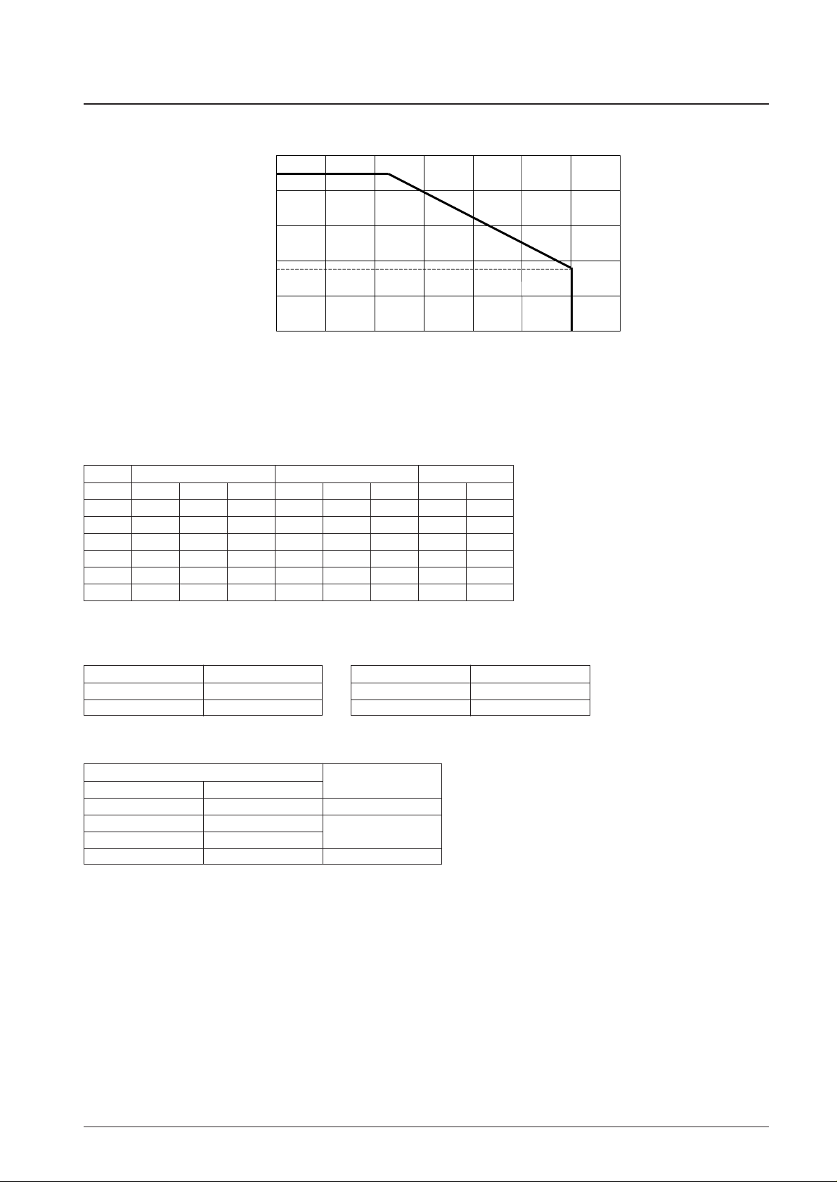
Pd max - Ta
0.36W
Ambient temperature, Ta - °C
Power dissipation, Pd max - W
0.9W Independent IC
Three-Phase logic Truth Table (IN = [H] indicates a condition in which IN+ > IN–.)
When S/S and PWMIN pins are not used, set the input to the L level voltage.
For HP output, pulsed output of Hall input IN1 (1-Hall output), 1/2 division output of 1 Hall, or synthetic output of three
phases of Hall input (three-Hall synthetic output) may be selected.
F/R = L F/R = H Output
IN1 IN2 IN3 IN1 IN2 IN3 PWM —
1 H L H L H L VH UL
2 H L L L H H WH UL
3 H H L L L H WH VL
4 L H L H L H UH VL
5 L H H H L L UH WL
6 L L H H H L VH WL
S/S pin
Input condition Condition
H or open Stop
L Start
PWMIN pin
Input condition Condition
H or open Output OFF
L Output ON
N1,N2 pin
Input condition
HP output
Pin N1 Pin N2
L L 1/2 division
L H or open
1 Hall
H or open L
H or open H or open Synthesis of three Halls
No. 7107-6/17
LB11824M
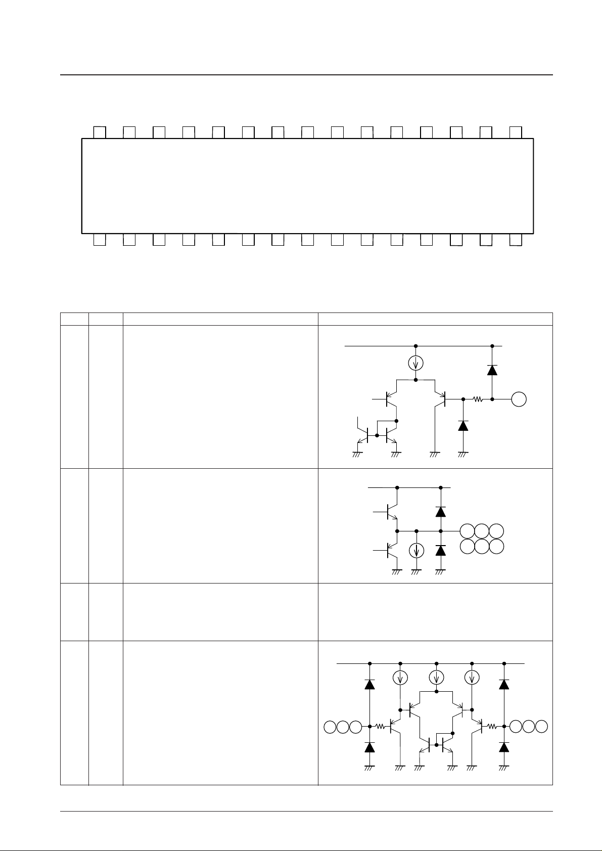
Pin Assignment
GND N2 HP F/R PWMIN
LB11824M
S/S
RF WH WL VH UH
CSD VCTL PWM
UL V
CC
1 IN1+ IN1–VL
N1
987654321 10 11 12 13 14 15
27 2628 24 2325 2129 2230
19 1820 1617
IN2+ IN2– IN3+ IN3– VREG
TOC 12REG V
CC
3 LVS VCC2
Pin Description
Pin No. Symbol Pin Description Equivalent circuit
Output current detection
Connect a resistor(Rf) between this pin and ground.
Set with the maximum output current IOUT = 0.5/Rf.
1 RF
VREG
5kΩ
1
Output pin (external TR drive output)
Duty control made on UH, VH, and WH sides.
2
4
6
3
5
7
WH
VH
UH
WL
VL
UL
VCC1
2 4 6
3 5 7
Power supply (output and Hall input blocks). Normally used
with the 12 V power supply. Connect to VCC2 and VREG
for application with the 5 V single power supply. Connect a
capacitor between this pin and GND for stabilization.
8
V
CC
1
Hall amplifier input.
IN+ > IN– is the input high state,
and the reverse is the input low state.
Connect a capacitor between the IN+ and IN– inputs if there
is noise in the Hall sensor signals.
9
10
11
12
13
14
IN1+
IN1–
IN2+
IN2–
IN3+
IN3–
VCC1
10 12 14
9 11 13
300Ω
300Ω
Continued on next page.
 Loading...