Ordering number :EN*6213A
63099RM (OT) No. 6213-1/10
Overview
The LB11817 is a spindle motor driver for use in slimshaped FDDs that use 5 V power supply.
Functions and Features
• Three-phase full-wave linear drive
• Low saturation voltage
• Built-in digital speed control
• Start/stop circuit (active low)
• Speed switching
• Current limiter
• Index processing circuit
• The index timing can be adjustment with a variable
resistor.
• Thermal protection circuit
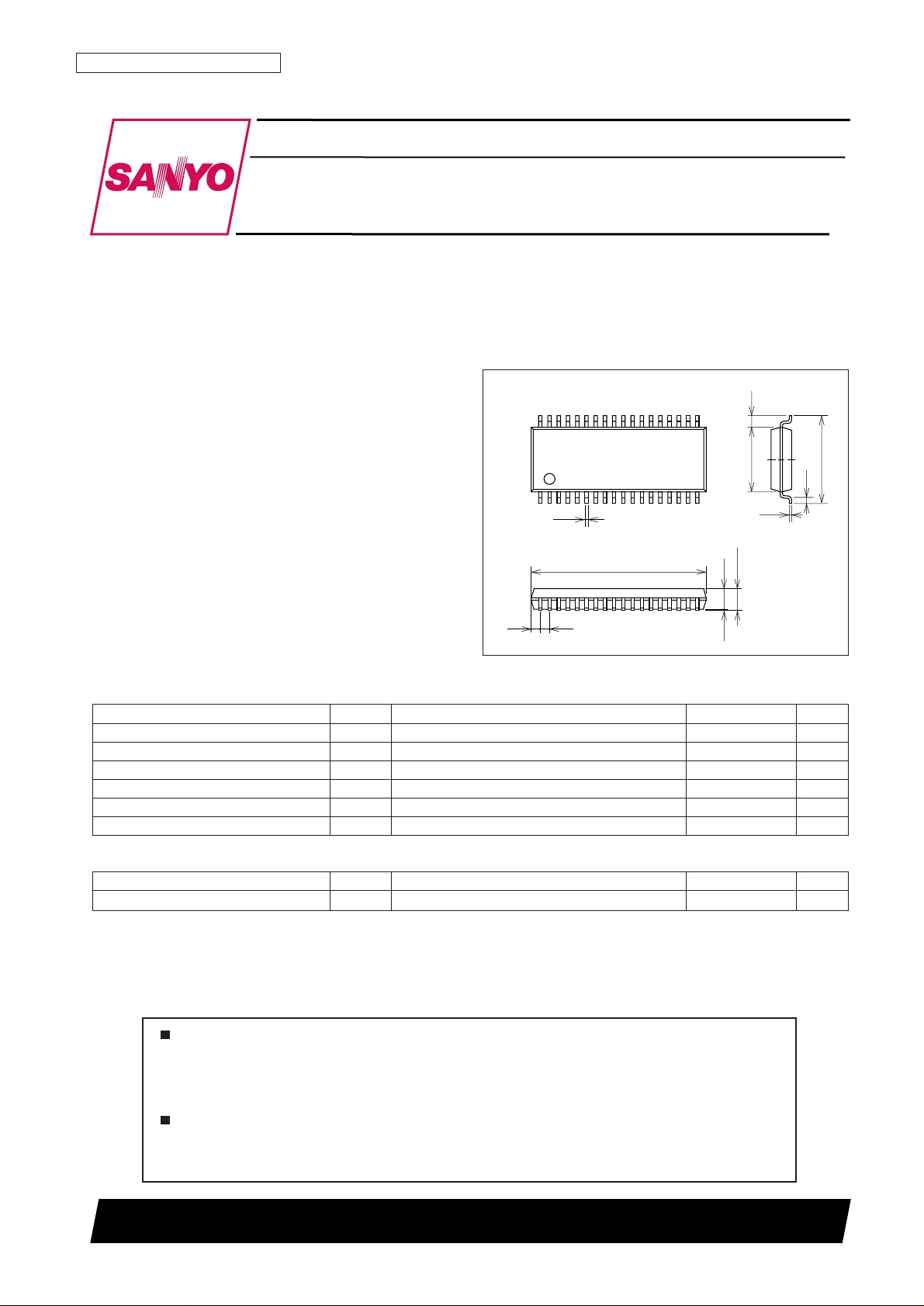
Package Dimensions
unit: mm
3247-SSOP36
1
36
18
19
0.8
15.2
0.5
7.6
0.20
0.30
0.8
5.6 1.0
(1.5)
1.8max
0.10
Preliminary
SANYO: SSOP36
[LB11817]
SANYO Electric Co.,Ltd. Semiconductor Company
TOKYO OFFICE Tokyo Bldg., 1-10, 1 Chome, Ueno, Taito-ku, TOKYO, 110-8534 JAPAN
Monolithic Digital IC
LB11817
Three-Phase Full-Wave Linear Drive
Any and all SANYO products described or contained herein do not have specifications that can handle
applications that require extremely high levels of reliability, such as life-support systems, aircraft’s
control systems, or other applications whose failure can be reasonably expected to result in serious
physical and/or material damage. Consult with your SANYO representative nearest you before using
any SANYO products described or contained herein in such applications.
SANYO assumes no responsibility for equipment failures that result from using products at values that
exceed, even momentarily, rated values (such as maximum ratings, operating condition ranges, or other
parameters) listed in products specifications of any and all SANYO products described or contained
herein.
Parameter Symbol Conditions Ratings Unit
Maximum supply voltage V
CC
max 7.0 V
Maximum output current I
O max
1t ≤ 0.5 s 1.5 A
Maximum steady-state output current I
O max
2 1.0 A
Allowable power dissipation 1 Pdmax1 Independent IC 0.6 W
Operating temperature Topr –20 to +80 °C
Storage temperature Tstg –40 to +150 °C
Specifications
Absolute Maximum Ratings at Ta = 25°C
Parameter Symbol Conditions Ratings Unit
Supply voltage V
CC
4.2 to 6.5 V
Allowable Operating Ranges at Ta = 25°C

No. 6213-2/10
LB11817
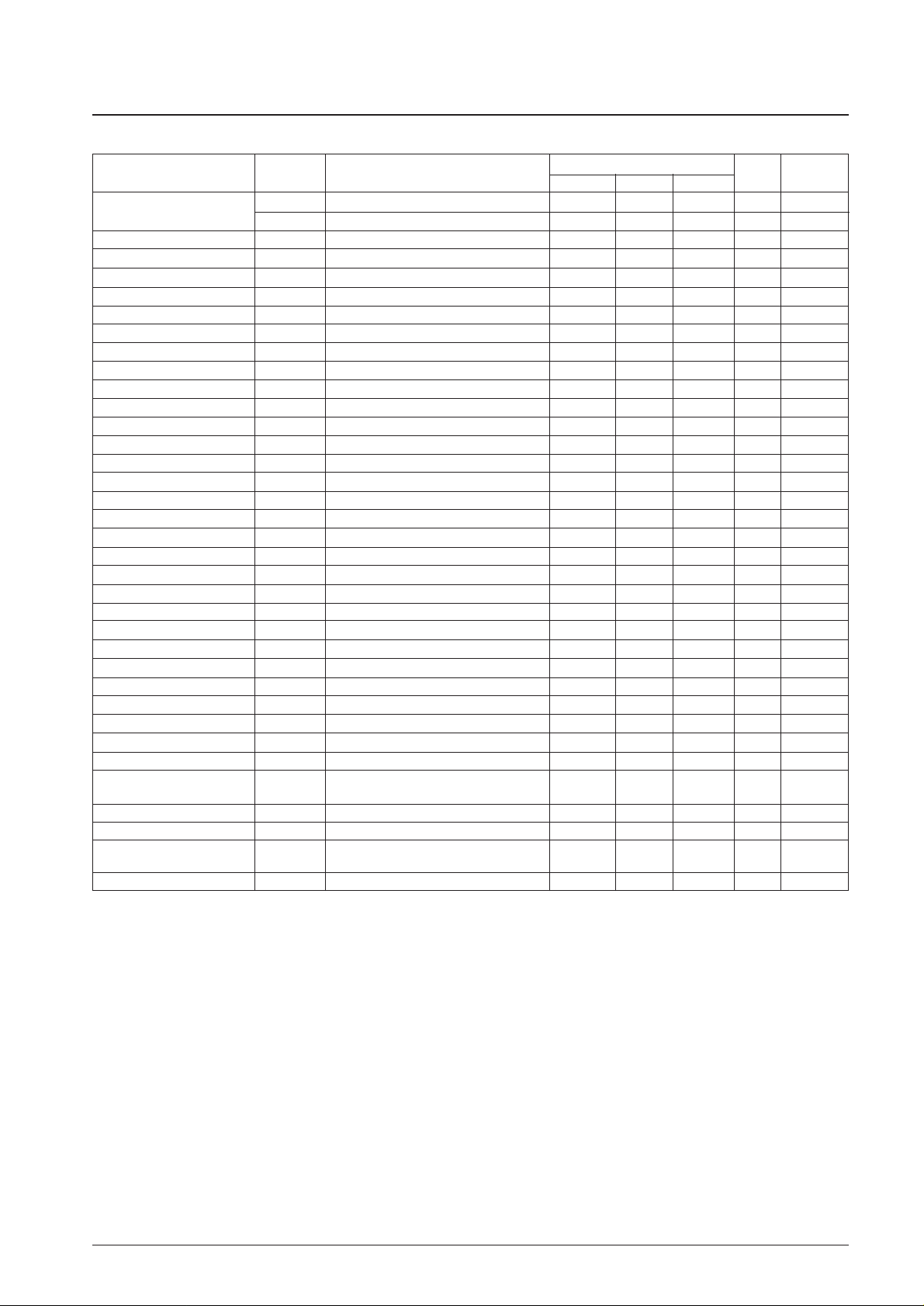
Electrical Characteristics at Ta = 25°C, VCC= 5 V
Note: * Items shown to be design target values are not measured.
Parameter Symbol Conditions
Ratings
Unit Note
min typ max
Current drain
I
CCO
S/S = 5 V (standby mode) 10 µA
I
CC
S/S = 0 V (normal operation) 17 25 mA
SL bias current I
SL
VSL= 0 V 10 µA
SL low-level input voltage V
SLL
0 1.0 V
SL high-level input voltage V
SLH
3.5 V
CC
V
S/S bias current I
S/S
150 230 µA
S/S low voltage V
S/SL
0 0.8 V
S/S high voltage V
S/SH
3.5 V
CC
V
Hall amplifier input bias current I
H
10 µA
Common-mode input voltage range
V
h
1.5
V
CC
– 1.0
V
Differential input voltage range V
dif
50 200 mVp-p
Hall bias output voltage V
HB
IH= 5 mA 0.5 0.8 1.1 V
Hall bias leakage current I
HBL
S/S = 5 V ±10 µA
Output saturation voltage V
sat
IO= 0.5 A sink+source 0.45 0.67 V
Output leakage current I
OL
1.0 mA
Current limiter V
lim
0.27 0.3 0.33 V
Control amplifier voltage gain G
C
–9 –7 –5 dB
Voltage gain inter-phase difference
∆G
C
±1 dB
V/I conversion source current I
+
91419µA
V/I conversion sink current I
–
–9 –14 –19 µA
V/I conversion current ratio I
+/I–
0.8 1.0 1.2
DSC buffer input current I
DSC
1.0 µA
FG amplifier voltage gain G
FG
48 dB *
FG offset amplifier input V
FG0
±10 mV *
FG amplifier internal reference voltage
V
FGB
2.2 2.5 2.8 V
FG Schmitt hysteresis ∆Vsh 50 mV *
Speed discriminator counts N 1041.5
Discriminator operating frequency
F
D
1.1 MHz *
Oscillator frequency range F
OSC
1.1 MHz *
Index output low-level voltage V
IDL
IO= 2 mA 0.4 V
Index output leakage current I
IDL
±10 µA
Index amplifier common-mode
V
ID
1.0
V
CC
– 1.0
V
input voltage range
Index input hysteresis ∆V
ID
25 mV
Boost voltage VP Ip = –5 mA 1.39 1.55 1.71 V
Thermal protection circuit
TSD 150 180 °C *
operating temperature
Hysteresis ∆TSD 40 °C *

No. 6213-3/10
LB11817
Pin Assignment
11
6
1
LB11817
19
22
23
26
27
30
29
35
36
I-
VR
I+
FG+
FG-
W-
W+
FGO
HB
V-
UU+
NC
NC
NC
UOUT
VOUT
PGND
WOUT
NC
D1
B1
B2
D2
V+
RF
VP
VCC
GND
DO
FC
CLK
SL
S/S
ID
TC
Top view
2
3
4
5
7
8
9
10
12
13
14
15
16
17
18
34
33
32
31
28
25
24
21
20
 Loading...