

Page 1
What is Laser Diode
The term laser is an acronym that stands for "Light Amplification by Stimulated Emission of
Radiation".
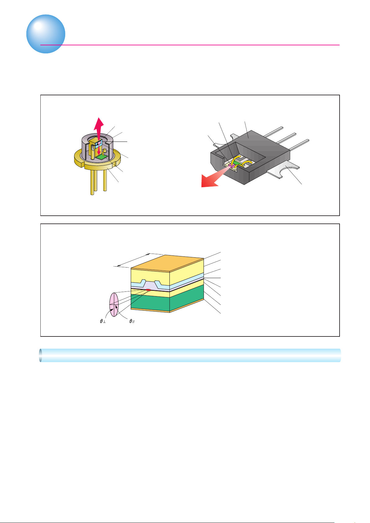
SANYO laser diode structure and basic element structure are listed below.
Laser diode structure
Can type
Cavity length
Window
Cap
Heatsink
Laser chip
PIN photodiode
Stem
PIN photodiode
Laser chip
Element structure
Electrode
Cap layer
Current blocking layer
Cladding layer
Active layer(MQW structure) *
Cladding layer
Substrate(Misoriented substrate)
Electrode
plastics
Heat radiation fin
Frame type
*MQW : Multiple Quantum Well
SANYO Laser Diodes Support Advanced Information Society
SANYO currently markets AlGaAs infrared laser diodes in the 780 – 830 nm wavelength, as well
as AlGaInP based red laser diodes in the 635 – 675 nm wavelength. SANYO realized 635 nm
AlGaInP laser diode for the first time in the world. The low operating current and high operating
temperature are realized by using misoriented substrate and MQW (Strain compensated) active
layer. With unique structures developed by SANYO, providing the following features, these laser
diodes are highly rated in a broad range of applications including compact discs, CD-R/RW, DVD
systems, bar code scanners, laser pointers and printers. SANYO laser diodes are also compatible
with multimedia and other new optical equipment on which advanced information societies in
future depend.
• A full line-up includes index guided short-wavelength, low-noise, high output power
• Long life and high reliability
• A stabilized fundamental transverse mode
• 9 mm, 5.6 mm diameter packages and frame type
• Pin connections compatible with various power supply systems
1
Page 2
Red Laser Diode
SANYO Red laser diode line-up
70
30
20
10
7
5
Output Power Po (mW)
3
DL-LS1035
*
DL-4038-
26
DL-4038- 31
DL-4038-021
DL-4148- 21
DL-3038-033/ 34
DL-3148- 33/ 34
DL-3038-013
DL-3148- 13
DL-3038-023
DL-3148- 23
635 650 670
DL-5147-041
DL-4147- 61
DVD-P/ROM
DL-3147- 65
DL-3147- 85
DL-3247- 65
DVD Frame Laser
NEW
DL-3107-165
DL-3147- 31
DL-3147-021
DVD-R/RW
DL-LS1027
*
655 675660
2 Beam (LBP)
DL-LS1018
*
DL-4039-011
DL-3039-011
DL-3149- 57
NEW
New product
Under development
*
Lasing Wavelength p (nm)
Summary of Features (Typ.
Absolute
Maximum Ratings
Light
Po
mW
7
3
5
10
10
25
35
7
12
3
5
5
7
7
7
7
12
7
30
50
5
7
10
Operating
Temperature
Topr
°C
–
+40
10 to
–
+40
10 to
–
+50
10 to
–
+40
10 to
–
+50
10 to
–
+40
10 to
–
+40
10 to
–
+40
10 to
–
+40
10 to
–
+40
10 to
–
+50
10 to
–
+40
10 to
–
+50
10 to
–
+70
10 to
–
+80
10 to
–
+70
10 to
–
+70
10 to
–
+70
10 to
–
+60
10 to
–
+70
10 to
–
+60
10 to
–
+60
10 to
–
+50
10 to
–
+60
10 to
Part No. Main Feature
DL-3038-013
DL-3038-023
DL-3038-033/ 34
DL-4038-021
DL-4038- 31
DL-4038- 26
DL-LS1035
*
DL-3148- 13
DL-4148- 21
DL-3148- 23
DL-3148- 33/ 34
DL-3147-021
DL-3147- 31
DL-3147- 65
DL-3147- 85
DL-3247- 65
DL-4147- 61
NEW
DL-3107-165
DL-5147-041
DL-LS1027
*
DL-3039-011
DL-3149- 57
DL-4039-011
DL-LS1018
*
Under development
*
5mW at 40°C
3mW at 40°C
5mW at 50°C
10mW at 40°C
10mW at 50°C
20mW at 40°C
30mW at 40°C
5mW at 40°C
10mW at 40°C
3mW at 40°C
5mW at 50°C
5mW at 40°C
5mW at 50°C
5mW at 70°C
5mW at 80°C
5mW at 70°C
10mW at 70°C
5mW at 70°C
30mW at 60°C
70mW at 70°C
5mW at 60°C
5mW at 60°C
10mW at 50°C
10mW ,2Beam
Output
10x2
)
Ratings
Po
5
3
5
10
10
20
30
5
10
3
5
5
5
5
5
5
10
5
30
50
5
5
10
10
Electro-Optical Characteristics
Threshold
Current
Ith
mA
30
20
30
35
35
40
50
30
40
20
40
30
25
25
25
25
30
20
45
45
30
25
40
40
Operating
Current
lop
mA nm ° °mW
45
25
40
55
55
70
90
45
60
25
55
45
35
35
35
35
50
30
80
110
45
40
60
60
Lasing
Wavelength
635
650
655
660
670
675
Monitor
Current
lm
mA
0.20
0.20
0.20
0.15
0.15
0.20
0.30
0.20
0.15
0.15
0.20
0.40
0.20
0.20
0.20
0.20
0.30
0.10
0.03
–
1.20
1.50
0.15
0.15
Beam Divergence
Parallel
***
Perpendicular
8.0
8.0
8.0
8.0
8.0
7.0
7.0
8.0
8.0
8.0
8.0
7.5
8.0
8.0
8.0
8.0
8.0
8.0
7.0
8.5
8.0
8.0
8.0
8.0
30
30
30
30
30
28
30
30
30
30
30
30
30
30
30
30
28
30
23
17
33
30
30
30
Tc = 25°C
Package
Dimension
Type
B
B
B
B
B
B
B
C
C
C
C
C
C
C
C
D
C
I
C
C
B
C
C
E
Pin
Connection
Type
I
I
I, III
I
I, III
I, III
I
I, III
I, III
I, III
I, III
I
I, III
I, II, III
I, II, III
I, II, III
I, II, III
II
I
IV
I
I, III
I
V
2
Page 3
Infrared Laser Diode
SANYO Infrared laser diode line-up
CD-R/RW
150
120
100
80
20
15
NEW
DL-7140-201K
*
DL-7140-201H
*
DL-7140-201S
*
DL-7240-201S
*
DL-4140-001S
2 Beam (LBP)
DL-LS2003
DL-8032-001
DL-7032-001
10
5
Output Power Po (mW)
DL-4034-154S
DL-3144-005S
Frame laser (CD-P/ROM)
DL-LS3004
NEW
DL-3150-133
*
Frame laser (CD-P/ROM)
DL-3150-103/105
3
DL-3144-007S
DL-3150-106/107
NEW
DL-3180-121
DL-LS3007
*
785 790 830
Lasing Wavelength p (nm)
Summary of Features (Typ.
Absolute
Maximum Ratings
Light
Po
mW
8
5
15
15x2
25
80
80
80
80
5
5
5
5
7
7
100
150
Operating
Temperature
Topr
°C
–
10 to +60
–
10 to +60
–
10 to +60
–
10 to +60
–
10 to +60
–
10 to +60
–
10 to +60
–
10 to +60
–
10 to +60
–
10 to +70
–
10 to +60
–
10 to +60
–
10 to +60
–
10 to +70
–
10 to +70
–
10 to +50
–
10 to +50
Part No. Main Feature
DL-3144-005S
DL-3144-007S
DL-4034-154S
DL-LS2003
*
DL-4140-001S
DL-7140-201S
DL-7240-201S
DL-7140-201H
NEW
DL-7140-201K
DL-3150-103/105
DL-3150-106/107
DL-3180-121
NEW
DL-LS3007
*
DL-LS3004
*
NEW
DL-3150-133
DL-7032-001
DL-8032-001
at the power of ratings Export control-regulations products Under development
*
Low droop
Low droop
10mW at 60°C
15mW 2Beam
20mW at 60°C
85mW(Pulse)
85mW(Pulse)
120mW(Pulse)
150mW(Pulse)
Frame Laser
Frame Laser
Frame Laser, Low current
Frame Laser, Low current
Frame Laser, 5mW
Frame Laser, 5mW
100mW at 50
150mW at 50
Output
°C
°C
)
Ratings
Po
5
3
10
15
20
70
70
70
70
3
3
3
3
5
5
100
150
Electro-Optical Characteristics
Current
Ith
mA
25
25
30
30
25
30
30
30
30
35
35
20
20
20
20
50
50
Operating
Current
lop
mA nm ° °mW
45
35
60
55
60
100
100
100
100
45
45
25
25
30
30
140
185
Threshold
*
Lasing
Wavelength
Monitor
Current
785
790
830
lm
mA
4.50
0.60
0.40
0.40
0.75
0.25
—
—
—
0.20
0.20
0.20
0.20
0.30
0.30
0.20
0.50
***
Parallel
Export control-regulations
products
Under development
*
New product
NEW
Pulse condition
*
Beam Divergence
Perpendicular
9.0
25
9.0
27
9.0
28
8.0
25
9.0
25
8.0
17
8.0
17
8.5
17
8.5
17
10.5
10.5
11.0
11.0
10.5
10.5
7.0
7.0
35
35
35
35
35
35
18
18
Tc = 25°C
Package
Dimension
Type
C
C
A
E
C
C
D
C
C
G/F
F/G
H
G
H
G
A
A
Pin
Connection
Type
I
I
II
V
I
III
IV
IV
IV
II
II
II
II
II
II
I
I
3
Page 4

Photograph
Can Type Laser Diodes
A
DL-8032
DL-7032
DL-4034
B C D E
DL-4039
DL-4038
DL-3039
DL-3038
DL-7140
DL-5147
DL-4148
DL-4147
DL-4140
DL-3149
DL-3148
DL-3147
DL-3144
DL-3247
DL-7240
DL-LS2003
*
DL-LS1018
*
ø9.0mm (Infrared) ø9.0mm (Red) D-shaped stem ø5.6mm (2 Beam)
ø5.6mm
Under development
*
Frame Type Laser Diodes
F G H I
DL-3150-103
DL-3150-107
DL-3150-105
DL-3150-106
DL-3150-133
*
DL-LS3007
DL-LS3004
*
DL-3180-121
DL-3107-165
*
Frame type (CD) Frame type (CD) Small frame type (CD) Frame type (DVD)
Under development
*
4
Page 5

Application
Application
Examples of Applied Systems
Applications Products
Laser Pointer
Point of guide
(Meeting, Exhibition
Sightseeing etc.)
Line Marker, Leveler
Reference for
construction
(For Parallel line,
For measurement
distance)
Bar-code Scanner
Merchandise control
DL-3038-013
DL-3038-023
DL-3147-021
DL-3148- 13
DL-3148- 23
DL-4038-021
DL-4038- 26
DL-3038- 33/-034
DL-3038- 33/-034
DL-3039-011
DL-3147- 31
DL-3148- 33/- 34
DL-3149- 57
DL-4038- 31
DL-4038- 31
DL-4148- 21
DL-LS1035
DL-4039-011
DL-4147- 61
DL-5147-041
DL-LS1035
DVD, DVD-R/RW
DVD
Laser
Beam
Printer
CD, CD-ROM, CD-R/RW
CD-R/RW
Optical Communication
Digital Versatile Disc
(DVD)-ROM, R/RW
Drive
Image printing
Word printing
Compact Disc(CD),
-ROM,R/RW Drive
Optical Communication
DVD DVD-R/RW
DL-3107-165
DL-3147- 65
DL-3147- 85
DL-3247- 65
DL-4147- 61
Red Laser Infrarde Laser
DL-3039-011
DL-3149- 57
DL-4039-011
DL-LS1018
CD, CD-ROM CD-R/RW
DL-3150-103/105
DL-3150-106/107
DL-3180-121
DL-3150-133
DL-LS3004
DL-LS3007
DL-7140-201S
DL-8032-001
DL-LS1027
DL-3144-005S
DL-3144-007S
DL-4034-154S
DL-LS2003
DL-4140-001S
DL-7140-201S
DL-7240-201S
DL-7140-201H
DL-7140-201K
DL-7032-001
5
Page 6
Key Technology
Strain compensated - MQW active layer
650~670nm Laser Diode
*
635nm Laser Diode (except DL-LS1035)
*
Quantum-barrier
Quantum-well
Quantum-barrier
Substrate
Quantum-well Tensile strain
Tensile strain
Compressive strain
Tensile strain
Compressive strainQuantum-barrier
Misoriented Substrate
[100]
[011]
[011]
Compressive strainQuantum-barrier
Substrate
Conventional Substrate
Misoriented Substrate
6
Page 7
Part Number Coding and Pin connection
Part Number Coding
DL-3 03 8-0 13
Laser diode series
Light output
Max.(mW)
3 :
4 :
5 :
6 :
7 :
8 :
7
20
40
50
100
150
Package dimension (mm)
03 : ø9.0
10 : Frame type(DVD)
14 : ø5.6
15 : Frame type(CD)
18 :
Small frame type(CD)
24 : D-shaped stem
Lasing wavelength (nm)
0 : 785–790
1 : 810
2 : 830
3 : 870
4 : 780
7 : 650–655
8 : 635
9 : 670–675
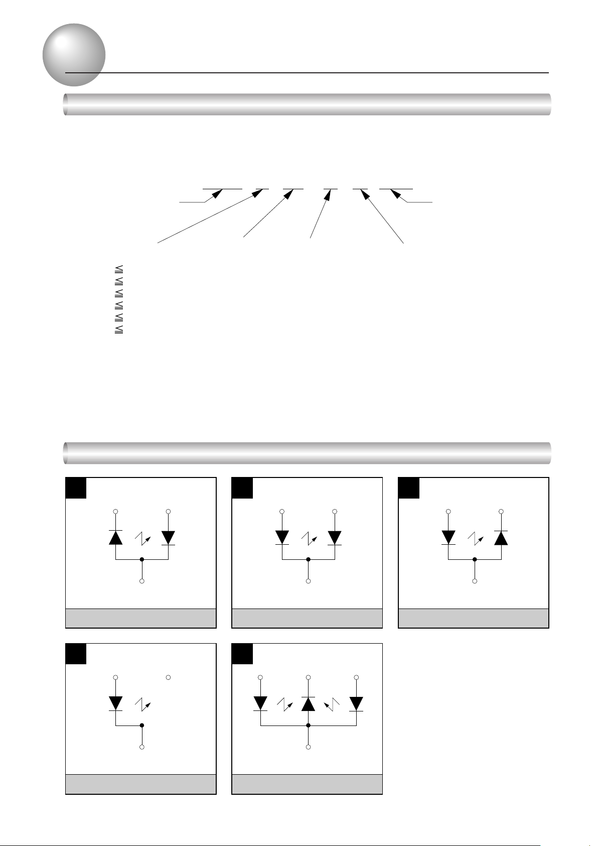
Pin connection
I II III
1 3
1 3
Suffix No.
Pin connection
0 : P-side down
(– power supply system)
1 : N-side down
(2 power supply systems)
2 : N-side down
(+ power supply system)
1 3
LD PD
2
– power supply system
IV
1 3 (NC)
LD
2
+ power supply system
no PD
LD PD
2
2 power supply system
V
1 3
LD1 LD2PD
2 beam + power supply system
2
4
LD PD
2
+ power supply system
7
Page 8

External appearance
External appearance dimensions
A CB
0
ø9.0–0.03
ø5.35
ø4.75±0.15
Effective window diameter 2.0min.
ø3.0
Effective window diameter 1.0min.
0
ø9.0–0.03
ø5.35
ø4.75±0.15
ø2.1
Tolerance : ±0.2
Unit : mm
0
ø5.6–0.025
ø4.4
ø3.55±0.1
Effective window diameter 1.0min.
ø1.6
1
3
1.0±0.1
LD facet
ø1.4max.
3–ø0.45±0.1
ø2.54
Top view
0.45±0.1
1.5±0.1
5.0±0.3
10±1.0
2.45±0.150.5max.
Pin No.
2
0.3
1 2 3
D E
0
ø5.6–0.025
ø4.4
ø3.55
Effective window diameter 0.6min.
ø1.6
2.45±0.150.5max.
Pin No.
1 3
2
0.3
1 2 3
Top view
1.0±0.1
0.45±0.1
LD facet
1.5±0.1
ø1.4max.
3–ø0.45±0.1
ø2.54
ø9.0mm stem (Red)
0
ø5.6–0.025
ø4.4
ø3.55±0.1
Effective window diameter 1.0min.
ø1.6
5.0±0.3
10±1.0
1.27±0.08
0.5max.
Pin No.
5.6mm ø stemø9.0mm stem (Infrared)
1 3
0.25
1 2 3
2
1.0±0.1
Top view
LD facet
ø1.4max.
3–ø0.45±0.1
ø2.0
0.4±0.1
1.2±0.1
3.5±0.5
6.5±1.0
2
1.270.5max.
Pin No.
1 3
4
1.0±0.1
1 4 3
Top view
LD facet
ø1.4max.
3–ø0.45±0.1
ø2.0
0.4±0.1
1.2±0.1
3.5±0.5
6.5±1.0
1.7±0.05
1.2
1.27±0.08
0.5max.
Pin No.
0.25
1 2 3
1.0±0.1
ø1.4max.
3–ø0.45±0.1
ø2.0
Top view
LD facet
0.4±0.1
1.2±0.1
3.5±0.5
6.5±1.0
D-shaped stem ø5.6mm stem (2 Beam)
8
Page 9

External appearance dimensions
F G
Tolerance : ±0.2
Unit : mm
1.9
3.4 1.85.0±0.5
0.7
0.7±0.12
R0.7
+0.1
0
1.4±0.12
3.0±0.1
6.4
2–0.4
3– 0.4±0.1
(
)
1.6
Pin No.
3.2
1.6
0
8.0
–0.1
4.0±0.12
3.7±0.15 3.0±0.15
4.2
3 2 1
2–C0.5
LD facet
2–R0.5
1.0
0.7
0.7±0.12
1.9
2–R0.7
3.4±0.12
3.7±0.15
+
0
1.4±0.12
3.4 1.85.0±0.5
3.0±0.1
6.4
2–0.4
3– 0.4±0.1
(
1.6
Pin No.
0.1
)
3 2 1
+0.1
0
0
+0.1
1.4
2
–
5
±
1
°
Frame type (CD) Frame type (CD)
6.8
1.6
4.2
3.2
0
–0.1
2–C0.5
LD facet
2
–
3
0
°
1.0
2
–
5
±
1
°
H I
0.21
1.41
0.2
2-0.3
2.0±0.15
0.5
1.75
1.37
1.75
4.0±0.1
2.87
3 2 1
ø3.3
0.6±0.15
LD facet
2-30
°
3.0
2.55
3.505.0±0.5
1.0
3-0.3
2-1.0 0.3
0.8
2.8
0.75±0.15
Pin No.
0.40.6
6.5 0.6
4.3
2-0.6
3.2
3-0.6
4.2
3.2
1.6
4.0
4.6
6.8±0.1
2.8
2 13
2-30
LD facet
0.9
°±
1°
2.4
0.8
2-5
°±
1°
1.4
5.5
1.0
2.9
0.6
Frame type (CD) Frame type (DVD)
9
Page 10

Definition of Feature
Absolute maximum ratings
Absolute maximum ratings are levels that can not be exceeded even momentarily
under any external conditions. The levels are stipulated in terms of case tempera
ture Tc = 25°C.
1. Light output power (PO)
This is maximum allowable output during
continuous operation. In the drive current
light output characteristics shown in the
figure on the right, there are no kinks or
bends under this light output power.
2. Reverse voltage (VR)
This is maximum allowable voltage with a
Output power P
reverse bias applied to the element. The
level is stipulated separately for a laser
diode and a photodiode.
3. Ambient operating temperature (Topr)
This is the maximum ambient temperature
in which the element can operate. The level is defined by case temperature of the
element.
Max. rating power
PO
Kink power
Forward current IF
Output power vs. Forward current (P–IF)
Non-linear
Kink
4. Ambient storage temperature (Tstg)
This is the maximum ambient temperature for element storage.
Electric optical characteristics
1. Threshold current (Ith)
Although P–IF curve distinguishes the LED
light emitting region A from the laser
oscillating region B, the current level that
triggers laser oscillating is the threshold
current. In actuality, Ith is defined as the
point where the straight line in B intersects
the X axis.
2. Rated light output power (Po)
This is recommended light output power
during continuous operation.
3. Operating current (Iop)
This is a current in the forward direction
that is required to generate rated light output power.
PO
Output power P
Output power vs. Forward current (P–IF)
LED
emitting region
B
A
Forward current IF
Laser
oscillating
region
lopIth
4. Monitor current (Im)
This is an output current of the photodiode at rated light output power.
10
Page 11

5. Differential efficiency (dP/dIop)
This is the increase in light output power per
unit of drive current. The amount is given by
the angle of the straight light output power
line with respect to forward current in the
laser oscillating range.
Definition of Feature
dP/dlop
dP
6. Lasing wavelength ( p)
This is peak lasing wavelength at rated
light output power. The lasing spectrum is
broadly classified as either a single mode
or a multi-mode as shown in the figure on
the right, and peak lasing wavelength is
defined by the maximum spectral intensity
in either mode.
Output power P
Forward current IF
Output power vs. Forward current (P–IF)
Single mode
Lasing spectrum
dlop
Multi mode
7. Beam divergence angle : Parallel ( ), Perpendicular( )
Light radiating from laser chip diverges as shown in the figure on the lower left. When the
light distribution is measured in the parallel (X axis) and perpendicular (Y axis) directions
with respect to the surface of the PN-junction on laser chip, (a) and (b) are shown in the
figure on the lower right. The beam divergence angle at 1/2 of the peak intensity of the light
distribution (full angle at half maximum) is defined as and .
Rear
PN-junction
Laser chip
Beam divergence
Front
1.0
Light
output power
0.5
Angle Angle
(a) (b)
Beam divergence ( , )
1.0
0.5
11
Page 12

Definition of Feature
8. Light axis off angle : Parallel ( ), Perpendicular ( )
This is expressed by a light axis shift with
respect to a reference surface. In a beam
divergent distribution of the parallel and
perpendicular directions as shown in the
figure on the right, shifts in both directions are
defined by (a - b)/2.
9. Light emission off center point (∆ X, ∆ Y, ∆ Z)
This is expressed by a shift in
the position of the light emitting
area. ∆ X and ∆ Y represent the
shift from the center of the
package, while ∆ Z represents a
shift with respect to stipulated
positions (a) from a reference
surface to the edge of a laser
diode (LD).
Top view
Light emission off center point (∆ X, ∆ Y, ∆ Z)
Light
output power
a
0
ZY
Side view
(a–b)/2
Light axis
off angle
Angle
LD facet
a
Reference plane
1.0
0.5
b
Light axis off angle ( , )
X
10. Astigmatism (As)
An astigmatism refers to a shift in focus position seen in the perpendicular and parallel
directions on the PN-junction surface of laser chip as shown in the figure on lower left.
11. Droop (∆ P)
This is the rate of light output power attenuation when a laser is driven by pulsed constant
current. The rate is defined by (A - B)/B x 100 % as shown in the figure on the lower right.
∆ P=(A–B)/Bx100%
A
Droop (∆ P)
600Hz
Duty : 10%
Duty : 90%
B
Time T
Laser chip
Astigmatism As
Focus position seen
in the parallel direction
Focus position seen
in the perpendicular
direction
Output power P
Laser beam
Astigmatism (As)
12
Page 13

Precautions for Use
Precautions for use
1. Temperature characteristics
Laser characteristics (wavelength, operating
current) vary with temperature, and variation
is more extreme at shorter wavelength. We
recommend installing an APC circuit to main
tain a constant output because operating
current varies significantly with temperature.
By the same token, laser reliability can be im
proved by designing products based on their
heat release characteristics. Since laser reli
ability falls off steeply at a higher tempera
ture, never allow the case to exceed the op
erating temperature range given in specifica
tions while a laser is in use.
25°C 50°C 70°C
Output power P
Forward current IF
Temperature characteristics of I-L curves
2. Thermal radiation
Make sure that a thermal radiating plate (W 30 x L 30 x t 5 mm) made of aluminum or
some other high thermal conducting materials is mounted to laser diode. The reliability
of laser diode is closely linked to junction temperature, so reliability rapidly declines at
a higher temperature. Do not overlook thermal radiation.
Thermal radiating plate
(Al or Cu)
3. Measuring light output power
Use a light power meter to measure light output
power of laser diodes. When measuring with APC
drive, set a power meter at an angle as shown in
the right figure so that a photodiode in a laser
diode is not exposed to reflected light from the
power meter.
Laser diode
Power meter
20°
13
Page 14

Precautions for Use
4. Absolute maximum ratings
Do not exceed, even momentarily, the maximum ratings.
When laser diode is driven in excess of the maximum ratings, it causes not only instant
breakdown or deterioration but also considerable reduction in reliability.
(1)
Laser diode may be damaged by surge current generated at power on-off operation.
Check on the transient characteristics of power supply to make sure that such surge
current does not exceed the maximum ratings.
(2)
The maximum ratings are specified by case temperature at 25˚C. Design should be
made well to work with temperature. As temperature goes up, power dissipation as
well as maximum light output power is reduced.
5. Soldering conditions
Maximum temperature is set at 260˚C and soldering time is within 3.0 seconds and
minimum clearance of 1.6 mm from the root of a lead is necessary.
6. Prevention of breakdown due to static electricity or surge current
Laser diode may be adversely affected by static electricity and surge current and,
consequently causes breakdown of element and reduction of reliability unless the
following cares are taken :
(1)
Power supply, installation and measuring equipment should be grounded. A noise
filter or noise-cut transformer is to be provided to power supply input utilized.
(2)
During operation, working clothes, hats and shoes should be static-protected when in
use.
Also, a workman body should be static-protected by use of an earth-band or the like
and grounded through high resistance (500 kΩ - 1MΩ ).
(3)
A soldering iron should be grounded to protect laser diodes from voltage leak.
(4)
Any container for carriage and storage should be static-protected.
(5)
Avoid using laser diodes at a place where high frequent surge current may be
generated as an inductive electric field gives breakdown or deterioration. (Avoid being
placed around fluorescent grow lamp, for example).
14
Soldering iron with surge protection
Static protected clothes
Conductive table mat
Grounded band
190
Humidifier
Conductive floor mat
1MΩ
Page 15

7. COD (Catastrophic Optical Damage) level
If current is flowing into the forward direction
and output continues to rise following a kink or
other deviation, then the laser eventually
reaches facet breakdown (COD) level where
the crystal at the facet melts due to the high
optical density. Special care must be taken in
the handling of red lasers because they may
continue to oscillate with a low power of 2 to 3
mW even after occuring facet breakdown.
There are several ways to tell whether an ele
ment is damaged or destroyed, such as
through a far field pattern or an increase in the
operating current. The life of a laser is signifi
cantly curtailed once the element is damaged,
so special care must be taken to avoid not
only excessing current when adjusting the out
put, but surge like static electricity as well.
Precautions for Use
COD level
Kink level
Output power P
Forward current IF
Output power vs. Forward current (P–IF)
Near field pattern
(A) Nomal laser
Near field pattern
(B) Damaged laser due to COD
Normal laser
Damaged laser
∆ lop
Po
Far field pattern
Damaged laser due to COD Output power vs. Forward current
Output Power (mW)
Forward current (mA)
lop1
lop2
15
Page 16

Precautions for Use
ESD data
(1) Measurement circuit
R=2MΩ
(2) Example of ESD data
100
80
60
40
Alive rate (%)
20
C=200pFV
AlGaInP Red laser diode
LD
(Machine model)
Judgment : ∆ lop 1.5mA
0
0
100
80
60
40
Alive rate (%)
20
0
0 20 40
20 40
60 80 100
Supplied voltage (V)
AlGaAs Infrared laser diode
60 80 100 120
Supplied voltage (V)
16
Page 17

8. Polarizing characteristics
Precautions for Use
Polarizing characteristics of red lasers vary
with distortions in the active layer. Conven
Y
635nm polarizing direction
tional infrared lasers as well as 650 to 675nm
lasers oscillate in the TE mode (polarizing di
rection parallel to the junction plane). As
such, special care must be taken when using
650–675nm, 780nm
X
polarizing direction
polarized optical parts with 635nm laser (ex
cept DL-LS1035) because it oscillates in the
TM mode (polarizing direction parpendicular
Top view of the stem
to the junction plane).
9. Package handling
(1)
Package must not be cut off, reworked nor deformed. Do not hold the cap of laser
diode tight, otherwise it may bring about cracks onto the window glass.
(2)
Do not touch the surface of the window glass. Any scratch or contamination may result
in reduction of optical characteristics.
(3)
Remove small contaminations on the surface softly using a cotton stick with a small
amount of methyl alcohol.
17
Page 18

Packaging
Packaging
192mm
43mm
1
Internal box
ESD
protective bag
(2tray / bag)
51mm
192mm
235mm
235mm
150
tray
Stem type Laser (300P)
100
Internal box
ESD
protective bag
(10tray / bag)
1
tray
18
Frame type Laser (1000P)
Page 19

Laser Drive System
Drive Circuit Recommendations
1. APC Circuit
GND
Im
R3
50k
V1
R4
4.7k
1/2 LA6358N
+
OP1
–
10µ
1k
2.2k
2.2k
+
5V
2.2k
V1
V2
1/2 LA6358N
–
OP2
+
47k5k
100k
470
1µ
2SD600
+
33µ
This APC drive circuit is used for type I pin connecting diagram.
When a laser diode (LD) emits light, light current (Im) proportionated to light output
power flows to a monitoring photodiode (PD) and a voltage V1 = Im (R3+R4) generates.
This voltage is sent by the op amp OP1 through a buffer to the op amp OP2.
Reference voltage V2 obtained from constant-voltage diode and volume switch is also
sent to the op amp OP2.
The op amp OP2 compares two voltages and then varies base current of output
transistor while controlling the current flowing to laser diode so that V1 = V2 is constantly
maintained. This is how constant light output power is obtained.
LDPD
R1
47µ
+
39
R2
10
Unit (Resistance : Ω Capacitance : F)
0.1µ
–
12V
Adjustment
Turn volume switch R3 as high as it will go, and set 5 kΩ volume switch so that V2 = 0.
(1)
Mount laser diode with power turned off.
(2)
Turn power on, and turn 5 kΩ volume switch to the center point while measuring light
(3)
output power with a light power meter. Here, light output power should be 1/2 of the
setting level. If difference from the setting level is significant, then turn off power and
adjust R3 and R4.
Turn volume switch R3 until light output power matches the setting level.
(4)
R1 – R4 setting procedure
Set light output range based on the data for laser diode characteristics and then use
(1)
the table below to determine proper operating current and monitoring output current
for light output power.
Light
output power
Pmax
Pmin
Operating
current
Imax
Imin
Monitoring
output current
Im max
Im min
19
Page 20

Laser Drive System
(2)
Set power resistance R1 and R2 for Imax based on table 1 used with the ACC circuit.
(3) After adjustments on the previous page, V2 will be about 1.7 volts.
Determine resistance R4 so that Immax x R4 = 1.7.
(4) Determine resistance R3 so that Immax x (R3 + R4) = 1.7. (Pmax = 4 mW and
Pmin = 1 mW when using 3 mW.)
2.APC Circuit
1/2 LA6358N
Im
PD
R3
1k
R4
100
+
–
OP1
10µ
1k
2.2k
+
2V
5k
5.6k
V1
V2
2k
–
OP2
+
1/2 LA6358N
33µ
+
470
100k
2SD600
1µ
+
47µ
R1
39
LD
Unit (Resistance : Ω Capacitance : F)
12V
0.1µ
GND
This drive circuit is used for type II pin connecting diagram. Operating principle
and adjustment procedure is exactly the same as that for APC circuit 1, except
that the resistance R3 and R4 settings are different.
R1 – R4 setting procedure
(1)
V2 in the circuit is about 0.26 volt, so determine resistance R4 so that Immax x R4 = 0.26.
(2)
Determine resistance R3 so that Immin x (R3 + R4) = 0.26. (Be sure to set R3 so that
voltage V1 is less than 0.5 volt because reverse bias is not applied to a photodiode).
3.APC Circuit
5V
1k
5k
2.2k
+
47k
2.2k2.2k
V2
V1
1/2 LA6358N
+
OP2
–
470
100k LD
33µ
2SB631
1µ
R2
10
47µ
+
0.1µ
R1
39
Unit (Resistance : Ω Capacitance : F)
R3
50k
Im
R4
4.7k
PD
–
OP1
+
1/2 LA6358N
+
10µ
This drive circuit is used for type III pin connecting diagram. The circuit is a version
of APC circuit 1 altered for reverse polarity characteristics and has the same
operating principle, adjustment procedure and resistance settings as APC circuit 1.
20
12V
GND
Page 21

Laser Drive System
4. APC Circuit
GND
+
C2
10µF
C1=1µ
TR1
2SC3383
0.6V
PD
R3
15kΩ
R4
5kΩ
LD
10kΩ
1kΩ
20µF
–
3V
(50Ω )
TR2
2SC3383
+
This is an example of an APC circuit for battery-powered Type I pin connection
circuits. It is ideally suited for a low-current DL-3148-023 The reference voltage
here is the voltage between the base and emitter of transistor TR1, and is normally
0.6 volts.
Since the absolute maximum rated power of the DL-3148-023 is 3 mW, the power
adjustment range for the circuit is between 0.5 and 2 mW. Resistors R3 and R4
used for adjusting power are set as outlined below.
Since Im is 0.12 mA at a maximum power of 2 mW, then R4 = VBE / Im = 0.6 / 0.12
= 5kΩ .
Then since R3 determines minimum optical output and Im is 0.03 mA with 0.5mW
of power, then R3 + R4 = VBE / Im = 0.6 / 0.03 = 20kΩ and R3 =15kΩ .
21
Page 22

Safety
The output light from laser diode is visible or invisible, and harmful to a human eye. Avoid looking at the output light of
laser diode directly or even indirectly through a lens while oscillating. When an optical axis is to be adjusted to a laser
beam and outer optical systems, a laser beam should be observed through an infrared TV camera or other equipment.
Particularly when the light is collimated or focused through a lens, safety glasses should be worn and care should be
taken to absolutely protect human eyes from the directly entering beam.
CAUTION – THE USE OF OPTICAL INSTRUMENTS WITH THIS PRODUCT WILL INCREASE EYE HAZARD.
Refer to IEC 825-1 and 21 CFR 1040.10 - 1040.11 as a radiation safety standard as to laser products.
LASER DIODE
Type :
Manufactured :
LASER DIODE
I S O
VISIBLE LASER RADIATIONAVOIDE DIRECT EXPOSURE TO BEAM
PEAK POWER 50 mW
WAVELENGTH 635-685 nm
CLASS IIIb LASER PRODUCT
AVOID EXPOSURE
-Visible laser radiation
is emitted from this aperture
INVISIBLE LASER RADIATIONAVOIDE DIRECT EXPOSURE TO BEAM
PEAK POWER 200 mW
WAVELENGTH 780-830 nm
CLASS IIIb LASER PRODUCT
This product complies with 21 CFR 1040.10
and 1040.11.
TOTTORI SANYO ELECTRIC CO., LTD.
LED DIVISION
5-318, Tachikawa, Tottori 680-8634 Japan
LASER DIODE
AVOID EXPOSURE
-Invisible laser radiation
is emitted from this aperture
Quality assurance system
LED Division of Tottori SANYO Electric Co., Ltd. takes pride in providing its customers
with the highest quality LED products possible. We are especially proud of the fact that all
LED products of our company have already obtained the verification of ISO 9001 in ac
cordance with IECQ (IEC Quality Assessment for Electronic Components). The produc
tion system is carried out in one continuous operation, including such processes as syn
thesis of compound semiconductors, single crystal growth and final display assembly. It
is our goal that, by making the best use of such production system, we develop quality
control activities which are supported by the verification of ISO, and offer the products in
100% conformance with our customers specifications.
Our quality assurance activities
for release of continually improving
new products are carried out re
flecting customers desires which
are constantly fed back into our
production lines. Our mass-pro
duction is controlled by standar
dized processes such as massproduction trial approval, a quality
control method to confirm the trial
products being made identical.
The guarantee shall be applied
only to the products delivered by
our company.
Environmental management system
Electronic Device Business Headquarters LED Division of Tottori Sanyo Electric Co.,
Ltd. has already obtained the verification of ISO 14001 in accordance with the assess
ment approval system of Environmental management system. The sphere of ISO 14001
are the development, design, manufacture and sales on the Optoelectoronic device.
45
 Loading...