

SANYO LA9241M Datasheet
Ordering number: EN 5564
Monolithic Linear IC
LA9241M
Analog Signal Processor (ASP)
for CD players
Overview
The LA9241M is an analog signal processing and servo control
bipolar IC designed for use in compact disc players; a compact
disc player can be configured by combining this IC with a
CD-DSP such as the LC78622E and LC78620E, with a small
number of additional components required.
Functions
I/V amplifier, RF amplifier (with AGC), SLC, APC, FE, TE
(with VCA and auto-balance function), focus servo amplifier
(with offset cancellation function), tracking servo amplifier
(with offset cancellation function), spindle servo amplifier
(with gain switching function), sled servo amplifier (with off
function), focus detection (DRF, FZD), track detection (HFL,
TES), defect detection, and shock detection.
Features
.
The following automatic adjustment functions are built in.
.
Focus offset auto cancel: FE (pin 20)
.
Tracking offset auto cancel: TE (pin 7)
.
EF balance auto adjustment
.
RF level AGC function
.
Tracking servo gain RF level following function
.
Focus search smoothing setting pin: FSC (pin 46)
.
EF balance adjustment variable range setting pin: (pin 47)
.
Focus search mode switching pin: (pin 55)
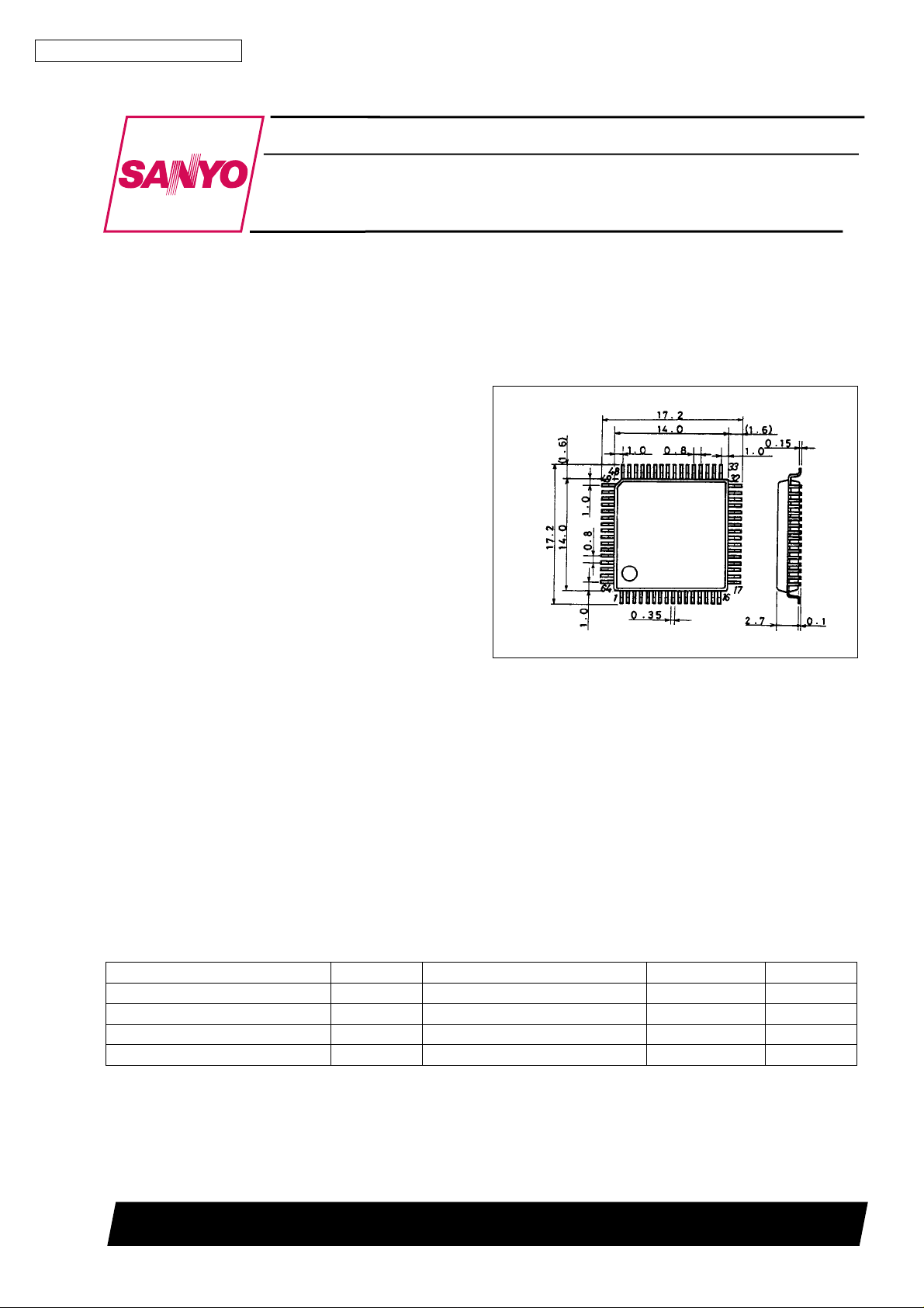
Package Dimensions
unit : mm
3159-QFP64E
[LA9241M]
SANYO : QFP64E
Specifications
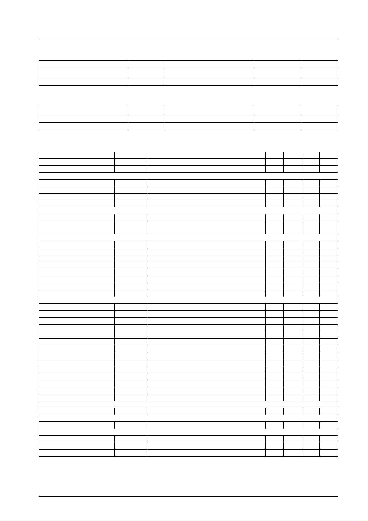
Maximum Ratings at Ta = 25°C, Pins 22, 45 = GND
Parameter Symbol Conditions Ratings Unit
Maximum supply voltage V
Allowable power dissipation Pd max 350 mW
Operating temperature Topr –25 to +75 °C
Storage temperature Tstg –40 to +150 °C
max Pin 56, 64 7 V
CC
SANYO Electric Co.,Ltd. Semiconductor Bussiness Headquarters
TOKYO OFFICE Tokyo Bldg., 1-10, 1 Chome, Ueno, Taito-ku, TOKYO, 110 JAPAN
13097HA(II)/83096HA(II) No.5564 - 1/21
LA9241M
Operating Conditions at Pins 22, 45 = GND
Parameter Symbol Conditions Ratings Unit
Recommended supply voltage V
Allowable operating supply voltage V
CC
op 3.2 to 5.5 V
CC
* Operating Supply Voltage at Limit of Operating Temperature at Pins 22, 45 = GND
Parameter Symbol Conditions Ratings Unit
Operating temperature Topr2 –10 to +75 °C
Allowable operating supply voltage V
op2 3.0 to 5.5 V
CC
Operating Characteristics at Ta = 25°C, Pins 22, 45 = GND, VCC(pins 56, 64) = 5 V
Parameter Symbol Conditions min typ max Unit
Current drain I
Reference voltage V
[Interface]
CE-Vth CEvth CE 0.8 V
CL-Vth CLvth CL 0.8 V
DAT-Vth DATvth DAT 0.8 V
Maximum CL frequency CLmax 500 kHz
[RF amplifier]
RFSM no signal voltage RFSMo 1.35 1.60 1.85 V
Minimum gain RFSM
[Focus amplifier]
FDO gain FD
FDO offset FDost Difference from reference voltage, servo on –170 0 +170 mV
Off time offset FDofost Difference from reference voltage, servo off –40 0 +40 mV
Offset adjustment step FEstep FE 3 mV
F search voltage H1 FSmax1 FDO, FSS = GND 0.8 V
F search voltage L1 FSmin1 FDO, FSS = GND –0.8 V
F search voltage H2 FSmax2 FDO, FSS = V
F search voltage L2 FSmin2 FDO, FSS = V
[Tracking amplifier]
TE gain MAX TE
TE gain MIN TE
TE−3 dB TEfc E: 1 MΩ-input 60 kHz
TO gain TO
TGL offset TGLost Servo on, TGL = H, TO –250 0 +250 mV
TGH offset TGHost TGL = L, difference from TGL offset, TO –50 0 +50 mV
THLD offset THLDost THLD mode, difference from TGL offset, TO –50 0 +50 mV
Off 1 offset OFF1ost TOFF = H –50 0 +50 mV
Off 2 offset OFF2ost TOFF2 off (IF) –50 0 +50 mV
Offset adjustment step TEstep TE 30 mV
Balance range H BAL-H ∆ Gain E/F input, TB=5V,TBC=open 3.5 dB
Balance range L BAL-L ∆ Gain E/F input, TB=0V,TBC=open –3.5 dB
TOFF-VTH TOFFvth 1.0 2.5 3.0 V
TGL-VTH TGLvth 1.0 2.5 3.0 V
[PH]
No signal voltage PHo Difference from RFSM –0.85 –0.65 –0.45 V
[BH]
No signal voltage BHo Difference from RFSM 0.45 0.65 0.85 V
[DRF]
Detection voltage DRFvth Difference from VR at RFSM –0.60 –0.35 –0.20 V
Output voltage H DRF-H 4.5 4.9 V
Output voltage L DRF-L 0 +0.5 V
CCO
REF
G
G
VCC1 (pin 64) + VCC2 (pin 56) 22 32 42 mA
VR 2.3 2.5 2.7 V
FIN1, FIN2:1MΩ-input, PH1=4V
min
G
freq = 200 kHz, RFSM
FIN2:1MΩ-input, FDO 3.5 5.0 6.5 dB
G
CC
CC
max f = 10 kHz, E: 1 MΩ-input, PH1=4V 6.0 7.5 9.0 dB
min f = 10 kHz, E: 1 MΩ-input, PH1=1V –0.5 +1.8 +4.0 dB
TH → TO gain, THLD mode 4.0 6.0 8.0 dB
G
5V
–14.0 –12.5 –11.0 dB
0.8 V
0V
Continued on next page.
No.5564 - 2/21
LA9241M
Continued from preceding page.
Parameter Symbol Conditions min typ max Unit
[FZD]
Detection voltage 1 FZD1 FE, difference from VR 0 +0.2 V
Detection voltage 2 FZD2 FE, difference from VR 0 V
[HFL]
Detection voltage HFLvth Difference from VR at RFSM –0.55 –0.4 –0.25 V
Output voltage H HFL-H 4.5 4.9 V
Output voltage L HFL-L 0 +0.5 V
[TES]
Detection voltage LH TES-LH TESI, difference from VR –0.15 –0.10 –0.05 V
Detection voltage HL TES-HL TESI, difference from VR 0.05 0.10 0.15 V
Output voltage H TES-H 4.5 4.9 V
Output voltage L TES-L 0 +0.5 V
[JP]
Output voltage H JP-H
Output voltage L JP-L
Difference from JP
–
JP
=5V,TO
Difference from JP
–
JP
=0V,TO
[Spindle amplifier]
Offset 12 SPD12ost Difference from VR at SPD, 12 cm mode –40 0 +40 mV
Offset 8 SPD8ost Difference from VR at SPD, 8 cm mode –40 0 +40 mV
Offset off SPDof Difference from VR at SPD, OFF mode –30 0 +30 mV
Output voltage H12 SPD-H12
Output voltage L12 SPD-L12
Output voltage H8 SPD-H8
Difference from offset-12, 12 cm mode
+
CV
=5V,CV–=0V
Difference from offset-12 , 12 cm mode
+
CV
=0V,CV–=5V
Difference from offset-8, 8 cm mode
+
CV
=5V,CV–=0V
[Sled amplifier]
SLEQ offset SLEQost Difference from TO at SLEQ –30 0 +30 mV
Offset SLD SLDost SLEQ = VR, Difference from VR –100 0 +100 mV
Offset off SLDof Off mode –40 0 +40 mV
Off VTH SLOFvth SLOF 1.0 1.4 2.0 V
[SLC]
No signal voltage SLCo SLC 2.25 2.5 2.75 V
[Shock]
No signal voltage SCIo SCI, difference from VR –40 0 +40 mV
Detection voltage H SCIvthH SCI, difference from VR 60 100 140 mV
Detection voltage L SCIvthL SCI, difference from VR –140 –100 –60 mV
[DEF]
Difference between LF2 voltage when RFSM =
Detection voltage DEFvth
3.5 V and DEF is detected and LF2 voltage when
RFSM = 3.5 V
Output voltage H DEF-H 4.5 4.9 V
Output voltage L DEF-L 0 +0.5 V
[APC]
Reference voltage LDS LDS voltage at which LDD=3V 160 190 220 mV
Off voltage LDDof LDD 3.9 4.3 4.6 V
+
=0V,JP–=0VatJP+=0V,
+
=0V,JP–=0VatJP+=5V,
0.35 0.5 0.65 V
–0.65 –0.5 –0.35 V
0.75 1.0 1.25 V
–1.25 –1.0 –0.75 V
0.35 0.5 0.65 V
0.20 0.35 0.50 V
No.5564 - 3/21
LA9241M
Pin Functions
Pin
Symbol Contents
No.
1 FIN2 Pickup photodiode connection pin. Added to FIN1 pin to generate the RF signal, subtracted from FIN1 pin to generate
2 FIN1 Pickup photodiode connection pin.
3 E Pickup photodiode connection pin. Subtracted from F pin to generate the TE signal.
4 F Pickup photodiode connection pin.
5 TB TE signal DC component input pin.
6TE
7 TE TE signal output pin.
8 TESI TES (Track Error Sense) comparator input pin. The TE signal is input through a bandpass filter.
9 SCI Shock detection input pin.
10 TH Tracking gain time constant setting pin.
11 TA TA amplifier output pin.
12 TD
13 TD Tracking phase compensation setting pin.
14 JP Tracking jump signal (kick pulse) amplitude setting pin.
15 TO Tracking control signal output pin.
16 FD Focusing control signal output pin.
17 FD
18 FA Pin for configuring the focusing phase compensation constant between the FD
19 FA
20 FE FE signal output pin.
21 FE
22 AGND Analog signal GND.
23 NC No connection
24 SP CV
25 SPG 12-cm spindle mode gain setting resistor connection pin.
26 SP
27 SPD Spindle control signal output pin.
28 SLEQ Sled phase compensation constant connection pin.
29 SLD Sled control signal output pin.
30 SL
31 SL
−
32 JP
+
33 JP
34 TGL Input pin for tracking gain control signal from DSP. Gain is low when TGL is high.
35 TOFF Input pin for tracking off control signal from DSP. Tracking servo is off when TOFF is high.
36 TES Output pin for TES signal to DSP.
37 HFL The High Frequency Level is used to determine whether the main beam is positioned over a bit or over the mirrored
38 SLOF Sled servo off control input pin
39 CV
40 CV
41 RFSM RF output pin.
42 RFS
43 SLC Slice Level Control is an output pin that controls the data slice level used by the DSP for the RF waveform.
44 SLI Input pin used by DSP for controlling the data slice level.
45 DGND Digital system GND pin.
46 FSC Focus search smoothing capacitor output pin.
47 TBC Tracking Balance Control; EF balance adjustment variable range setting pin
48 NC No connection
49 DEF Disc defect detection output pin.
50 CLK Reference clock input pin. 4.23 MHz signal from the DSP is input.
51 CL Microprocessor command clock input pin.
the FE signal.
−
Pin which connects the TE signal gain setting resistor between this pin and TE pin.
−
Pin for configuring the tracking phase compensation constant between the TD and VR pins.
−
Pin for configuring the focusing phase compensation constant between the FD and FA pins.
−
Pin for configuring the focusing phase compensation constant between the FA and FE pins.
−
Pin which connects the FE signal gain setting resistor between this pin and FE pin.
+
and CV−pins input signal single-end output.
−
Spindle phase compensation constant connection pin, along with the SPD pin.
−
Input pin for sled movement signal from microprocessor.
+
Input pin for sled movement signal from microprocessor.
Input pin for tracking jump signal from DSP.
Input pin for tracking jump signal from DSP.
surface.
−
Input pin for CLV error signal from DSP.
+
Input pin for CLV error signal from DSP.
−
RF gain setting and EFM signal 3T compensation constant setting pin, along with the RFSM pin.
−
and FA−pins.
Continued on next page.
No.5564 - 4/21
LA9241M
Continued from preceding page.
Pin
Symbol Contents
No.
52 DAT Microprocessor command data input pin.
53 CE Microprocessor command chip enable input pin.
54 DRF RF level detection output (Detect RF).
55 FSS Focus Search Select; focus search mode (± search/+search vs. the reference voltage) switching pin
56
V
2 Servo system and digital system VCCpin.
CC
57 REFI By-pass capacitor connection pin for reference voltage.
58 VR Reference voltage output pin.
59 LF2 Disc defect detection time constant setting pin.
60 PH1 RF signal peak hold capacitor connection pin.
61 BH1 RF signal bottom hold capacitor connection pin.
62 LDD APC circuit output pin.
63 LDS APC circuit input pin.
64
V
1 RF system VCCpin.
CC
No.5564 - 5/21
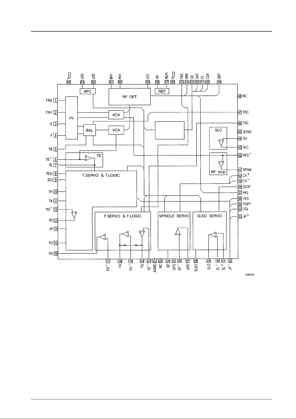
Equivalent Circuit Block Diagram
LA9241M
Microcontroller
INTERFACE
No.5564 - 6/21
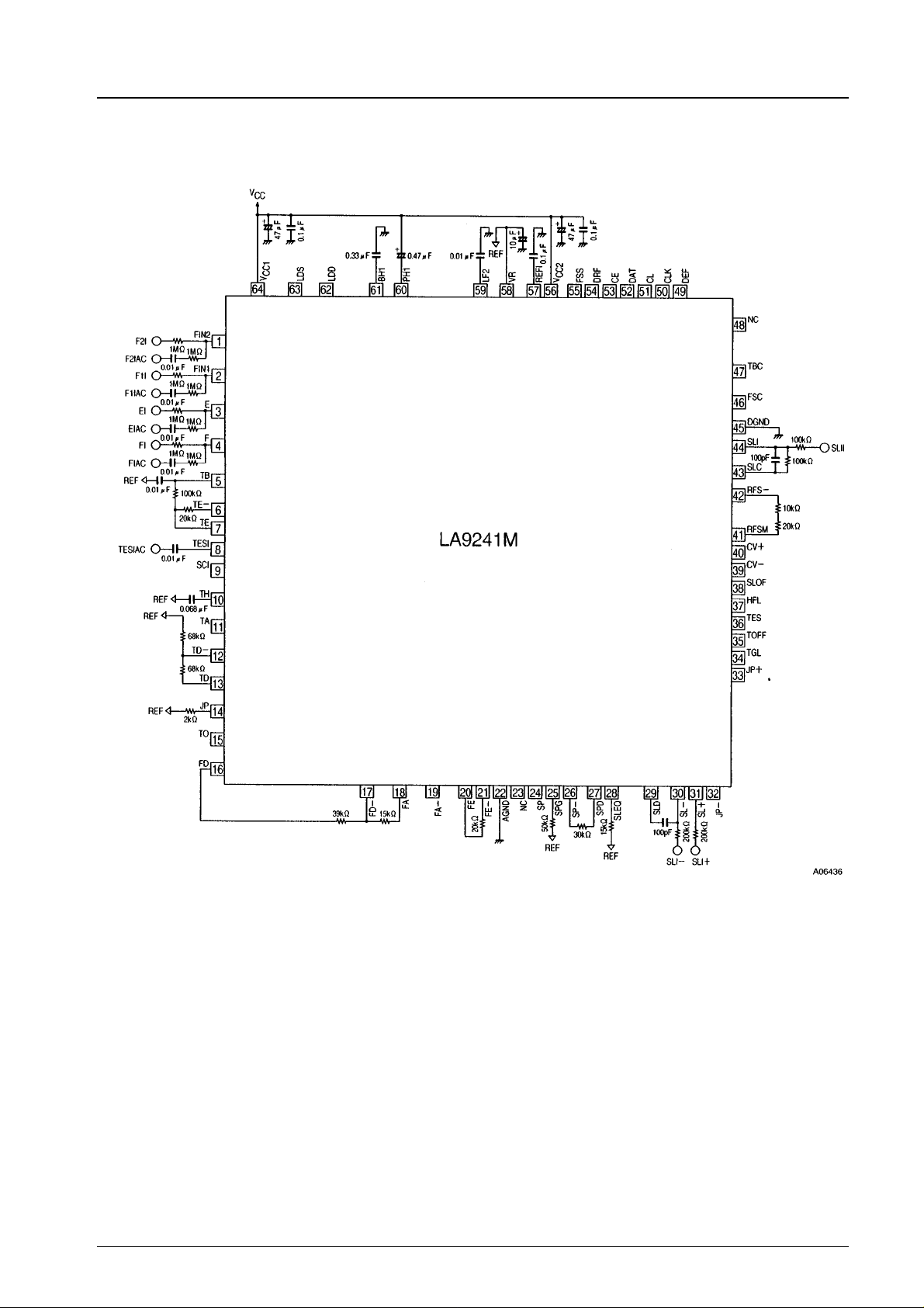
Test Circuit
LA9241M
No.5564 - 7/21
 Loading...