

Page 1
Monolithic Linear IC
Ordering number : EN4930
52095TH (OT) No. 4930-1/10
SANYO Electric Co.,Ltd. Semiconductor Bussiness Headquarters
TOKYO OFFICE Tokyo Bldg., 1-10, 1 Chome, Ueno, Taito-ku, TOKYO, 110-8534 JAPAN
Double-Conversion Narrow-Band
FM IF System
LA8670M
Overview
The LA8670M is a narrow band FM IF system for use in
communication equipment. In addition to the functions
required for FM reception, the LA8670M provides a rich
set of additional functions including noise detection and
field strength detection, and is thus optimal for cordless
telephones.
Functions
• First mixer, first local oscillator, first local oscillator
buffer output, second mixer, second local oscillator
• IF amplifier, limiter, quadrature detector
• Signal meter
• Noise detector, noise amplifier, noise wave detector,
Schmitt trigger
Features
• Low voltage operation: V
CC OP
= 1.8 to 6 V
• Signal meter linear over a wide range (70 dB typical)
• High sensitivity, high intercept point
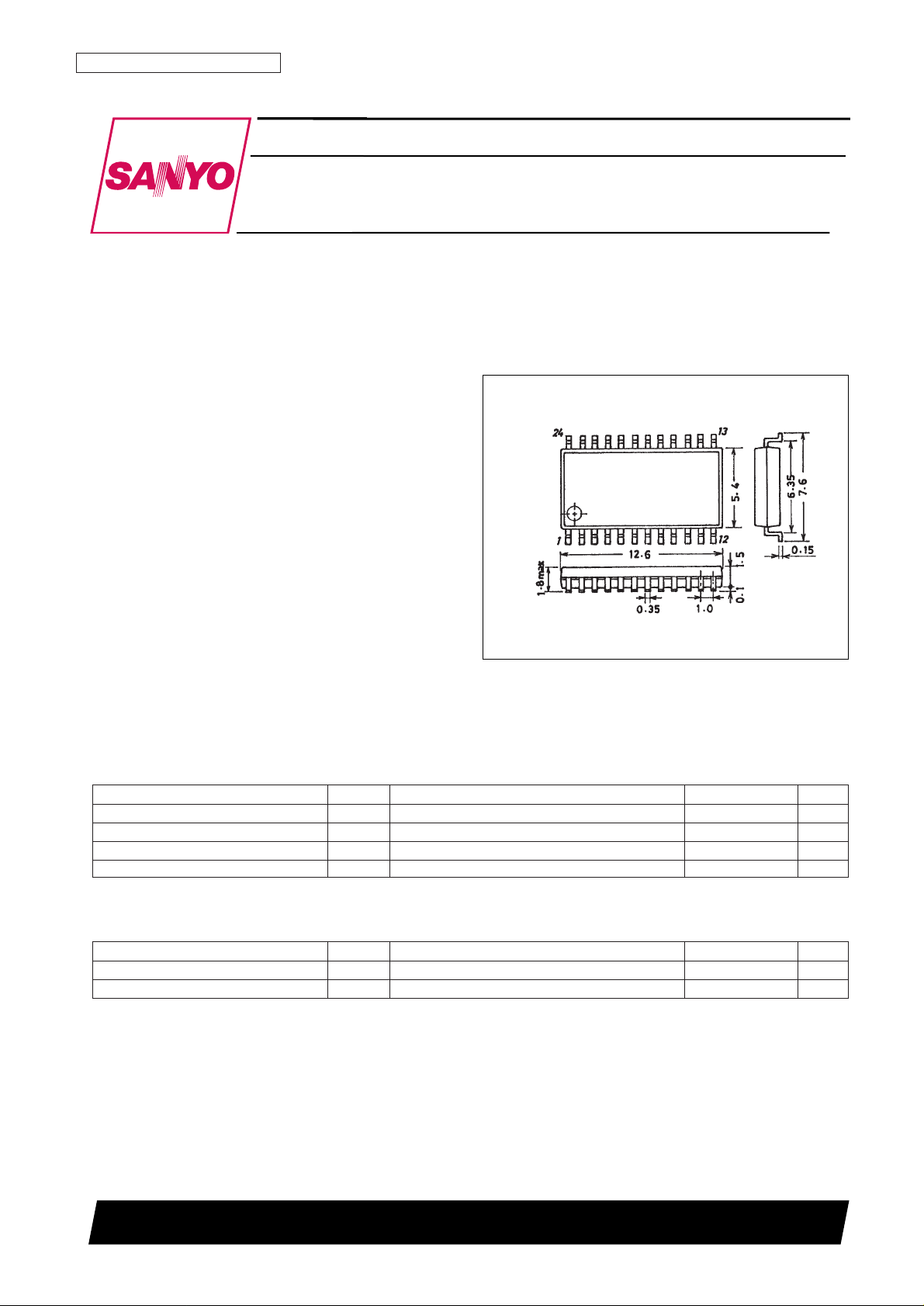
Package Dimensions
unit: mm
3112-MFP24S
Specifications
Maximum Ratings at Ta = 25°C
Operating Conditions at Ta = 25°C
Parameter Symbol Conditions Ratings Unit
Maximum supply voltage V
CC
max 7.0 V
Allowable power dissipation Pd max Ta ≤ 75°C 150 mW
Operating temperature Topr –20 to +75 °C
Storage temperature Tstg –40 to +125 °C
Parameter Symbol Conditions Ratings Unit
Recommended supply voltage V
CC
3.0 V
Operating supply voltage V
CC OP
1.8 to 6.0 V
[LA8670M]
SANYO:MFP24S
Page 2

Operating Characteristics at Ta = 25°C, VCC= 3 V, fC(MIX) = 49.830 MHz, fmod = 1 kHz, ∆f = ±3 kHz
Note: AC levels are all indicated for open (EMF) circuits.
No. 4930-2/10
LA8670M
Parameter Symbol Conditions min typ max Unit
Quiescent current I
CCO
No input 7.3 9.5 mA
Mixer intercept point Ip3 First mixer –4.8 dBm
12 dB sensitivity 12dB S/N No input matching 3.2 5.0 dBµ
Demodulator output V
O
Vin = 80 dBµ 143 180 227 mVrms
Signal-to-noise ratio S/N No modulation, Vin = 80 dBµ 60 67 dB
AM rejection ratio AMR AM 30% modulation 35 43 dB
Total harmonic distortion THD Vin = 80 dBµ 2.2 3.0 %
V
SM (1)
Vin = 0 dBµ 0.05 0.30 0.65 V
Signal meter output V
SM (2)
Vin = 40 dBµ 0.60 0.90 1.40 V
V
SM (3)
Vin = 80 dBµ 1.05 1.40 1.85 V
Noise detector output
V
ND (1)
fi = 40 kHz, Vi = –50 dBV 0.10 0.25 V
V
ND (2)
fi = 40 kHz, Vi = –30 dBV 1.10 1.40 1.70 V
Noise detector level
V
14 (1)
Schmitt on 0.53 0.63 0.73 V
V
14 (2)
Schmitt off 0.33 0.43 0.53 V
Schmitt output level
V
SH (1)V14
= 0.8 V 0.3 V
V
SH (2)V14
= 0.2 V 2.8 V
Mixer conversion gain
G
M1
First mixer 19 dB
G
M2
Second mixer 24 dB
Mixer input frequency 90 MHz
Mixer input resistance
First mixer 5 kΩ
Second mixer 330 Ω
Mixer output resistance
First mixer 330 Ω
Second mixer 2.0 kΩ
FM detector output impedance 520 Ω
Page 3
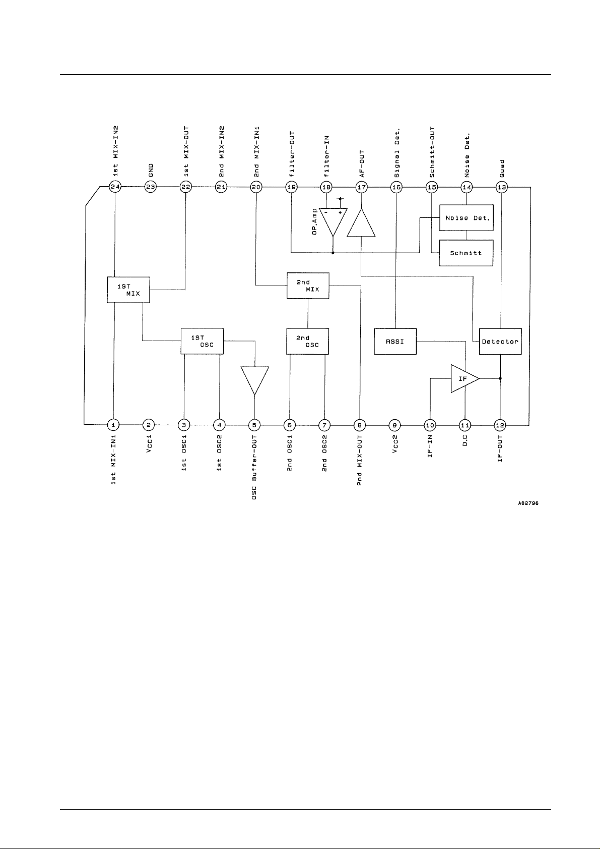
Equivalent Circuit Block Diagram
No. 4930-3/10
LA8670M
Page 4

Test Circuit
No. 4930-4/10
LA8670M
Page 5

Sample Application Circuit
No. 4930-5/10
LA8670M
Page 6

Pin Functions
No. 4930-6/10
LA8670M
Pin No. Symbol Internal equivalent circuit Note
24
1
2
3
4
5
6
7
8
9
10
11
12
1st MIX-IN 2
1st MIX-IN 1
V
CC
1
1st OSC 1
1st OSC 2
OSC Buffer-OUT
2nd OSC 1
2nd OSC 2
2nd MIX-OUT
VCC2
IF-IN
D.C
IF-OUT
First mixer inputs
Power supply for the first mixer
Local oscillator inputs
Local oscillator buffer output
Local oscillator inputs
When external insertion is used, input the signal to
pin 6 and leave pin 7 open.
Second mixer output
Power supply
IF amplifier input
IF amplifier DC feedback
Limiter amplifier output
Continued on next page.
Page 7

Continued from preceding page.
No. 4930-7/10
LA8670M
Continued on next page.
Pin No. Symbol Internal equivalent circuit Note
13
14
15
16
17
18
19
20
21
Quad.
Noise det.
Schmitt-OUT
Signal DET.
AF-OUT
Filter-IN
Filter-OUT
2nd MIX-IN 1
2nd MIX-IN 2
Discriminator connection
Noise detector
Noise Schmitt output
Field strength signal output
FM detector output
Noise filter input
Noise filter output
Second mixer input
Page 8

Continued from preceding page.
No. 4930-8/10
LA8670M
Pin No. Symbol Internal equivalent circuit Note
22
23
1st MIX-OUT
GND
First mixer output
Ground
Page 9

No. 4930-9/10
LA8670M
Page 10

PS No. 4930-10/10
LA8670M
This catalog provide information as of May, 1995. Specifications and information herein are subject to change
without notice.
■ No products described or contained herein are intended for use in surgical implants, life-support systems, aerospace
equipment, nuclear power control systems, vehicles, disaster/crime-prevention equipment and the like, the failure of
which may directly or indirectly cause injury, death or property loss.
■ Anyone purchasing any products described or contained herein for an above-mentioned use shall:
➀ Accept full responsibility and indemnify and defend SANYO ELECTRIC CO., LTD., its affiliates, subsidiaries and
distributors and all their officers and employees, jointly and severally, against any and all claims and litigation and all
damages, cost and expenses associated with such use:
➁ Not impose any responsibility for any fault or negligence which may be cited in any such claim or litigation on
SANYO ELECTRIC CO., LTD., its affiliates, subsidiaries and distributors or any of their officers and employees
jointly or severally.
■ Information (including circuit diagrams and circuit parameters) herein is for example only; it is not guaranteed for
volume production. SANYO believes information herein is accurate and reliable, but no guarantees are made or implied
regarding its use or any infringements of intellectual property rights or other rights of third parties.
 Loading...