

SANYO LA8638V Datasheet
Overview
The LA8638V provides dynamic range expansion, noise
suppression for enhancing the quality of audio signals in
cordless telephones and other communications systems.
This single chip provides the functions that make it ideal
for cordless telephones: a compressor with a logarithmic
compression ratio of 1/2, expander with a logarithmic
expansion ratio of 2, splatter filter, microphone amplifier,
BTL amplifier, waveform shaper for the receiving signal,
muting for both receiving and transmitting signals, and
standby operation.
Functions
• Transmitter circuits: compressor, microphone amplifier,
limiter (IDC), muting, output level changes to userspecified levels, and splatter filter
• Receiver circuits: expander, buffer amplifier for filters,
muting, output level changes to user-specified levels,
and BTL amplifier
• Other circuits: waveform shaper for the receiving signal
and standby operation
Features
• Full processing of baseband signals for both receiving
and transmitting signals
• Built-in BTL receiver amplifier for driving a ceramic
speaker with a load of 2 kΩ
• Standby operation that conserves battery power during
intermittent reception by disabling all but the waveform
shaper for the receiving signal
• Built-in splatter filter with user-specified fc
• Low-voltage operation (1.8 V to 5.5 V)
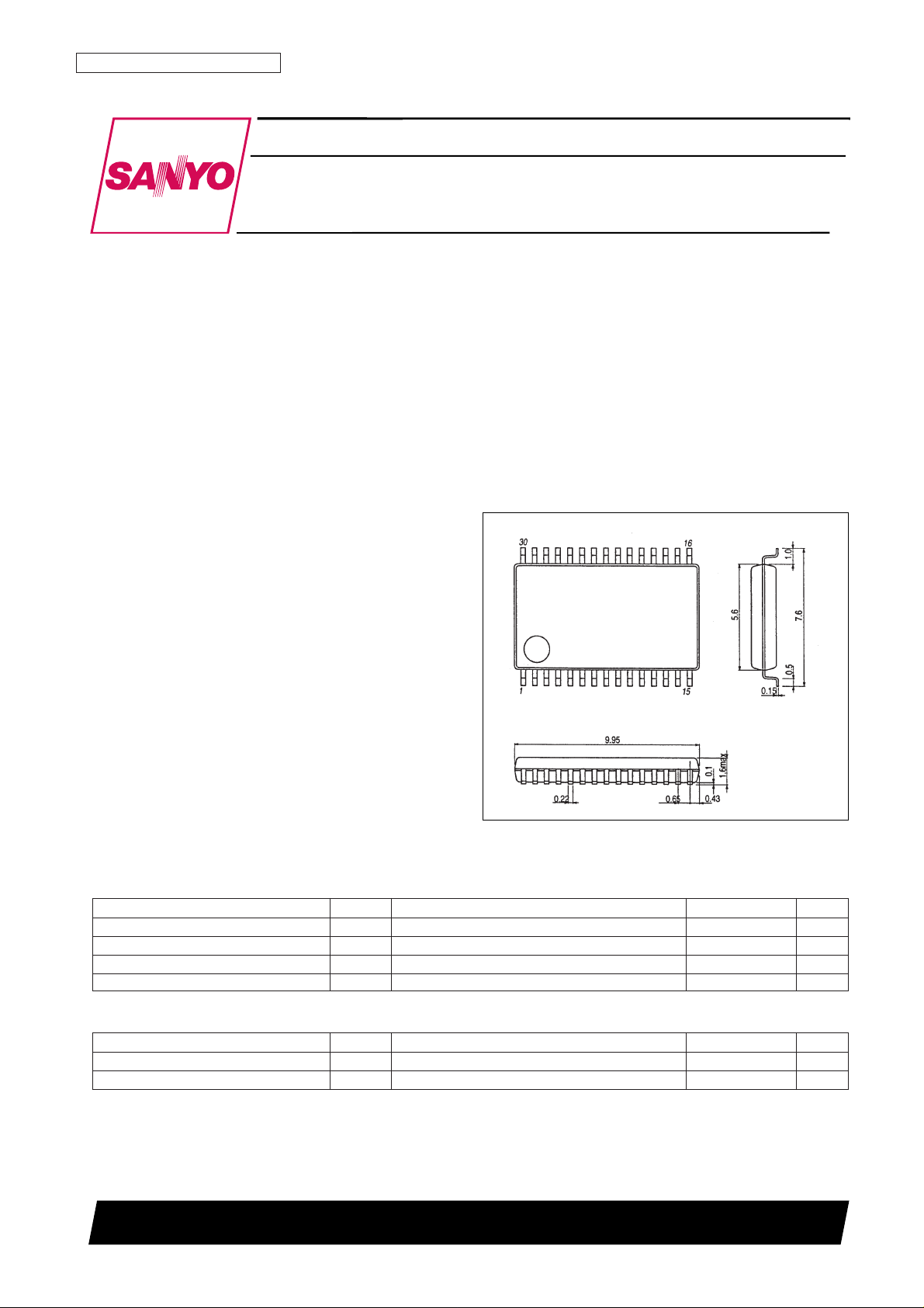
Package Dimensions
unit: mm
3191-SSOP30
Monolithic Linear IC
40398RM (OT) No. 5776-1/16
SANYO: SSOP30
[LA8638V]
SANYO Electric Co.,Ltd. Semiconductor Bussiness Headquarters
TOKYO OFFICE Tokyo Bldg., 1-10, 1 Chome, Ueno, Taito-ku, TOKYO, 110-8534 JAPAN
Low-voltage Compander IC
for Cordless Telephones
LA8638V
Ordering number : EN5776
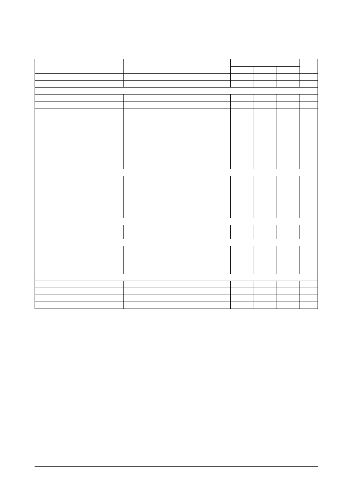
Parameter Symbol Conditions Ratings Unit
Maximum power supply voltage V
CC
max 7.0 V
Maximum power dissipation Pd max Ta ≤ 75°C 100 mW
Operating temperature Topr –20 to +75 °C
Storage temperature Tstg –40 to +125 °C
Specifications
Maximum Ratings at Ta = 25°C
Parameter Symbol Conditions Ratings Unit
Recommended power supply voltage V
CC
2.4 V
Operating power supply voltage range V
CC
op 1.8 to 5.5 V
Operating Conditions at Ta = 25°C
No. 5776-2/16
LA8638V
Parameter Symbol Conditions
Ratings
Unit
min typ max
Current drain with no signal I
CCO
No signal 3.0 5.4 7.6 mA
Standby current I
STBY
Standby mode, No signal 0.4 0.7 0.95 mA
[Transmitter block] V
inrefc
= –60 dBV = 0 dB, microphone amplifier gain = 40 dB, RL= 15 kΩ
Output level V
O
c VIN= Vinrefc = 0 dB –18.1 –16.1 –14.1 dBV
Gain change level G
C
c VIN= –10 dB 3.5 4.0 4.4 dB
Gain error G
E
c VIN= –40 dB –2.0 –0.7 +1.0 dB
Total harmonic distortion THDc V
IN
= 0 dB 0.45 1.0 %
Output noise voltage V
NO
c Rg = 620Ω, f = 20 to 20 kHz 1.8 4.5 mVrms
Limiting voltage V
LT
VIN= +30 dB, 1 kHz BPF 0.88 1.05 1.23 Vp-p
Microphone amplifier maximum voltage gain VG max 40 46 dB
Low pass filter attenuation Lalt
f
IN
= 5 kHz; fifth-order Butterworth function
12.0 16.5 25.0 dB
filter (fc = 3.35 kHz)
Muting attenuation ATTc V
IN
= +30 dB, 1 kHz BPF –83 –65 dBV
Crosstalk level CTc RX—V
IN
= –10 dBV, 1 kHz BPF –61 –50 dBV
[Receiver block] V
inrefe
= –20 dBV = 0 dB, RL= 15 kΩ
Output level V
O
e VIN= V
inrefe
= 0 dB –18.8 –16.3 –13.8 dBV
Gain change level G
C
e VIN= 0 dB 6.0 7.1 8.4 dB
Gain error G
E
e VIN= –30 dB –1.5 +0.3 +2.0 dB
Output noise voltage V
NO
e Rg = 620 Ω, f = 20 to 20 kHz 50 100 µVrms
Muting attenuation ATTe V
IN
= +10 dB, 1 kHz BPF –100 –80 dBV
Crosstalk level CTe TX—V
IN
= –40 dBV, 1 kHz BPF –83 –65 dBV
[BTL amplifier] R
L
= 2 kΩ
Maximum output voltage V
O
btl THD = 3% 3.2 4.2 Vp-p
Total harmonic distortion THDbtl V
IN
= –5 dBV 0.4 1.0 %
[Data shaper] V
IN
= –20 dBV, RL= 100 kΩ
Duty factor DUTY 43 50 57 %
Dead zone UNSN –39.0 –34.5 –30.0 dBV
Output “H” level V
H
2.2 2.38 V
Output “L” level V
L
0.12 0.3 V
[Digital input characteristics]
Input “H” level 1 V
IH
1 Pins 17, 18, 20, and 22 0.6 V
CC
V
Input “L” level 1 V
IL
2 Pins 17, 18, 20, and 22 0.25 V
CC
V
Input “H” level 2 V
IH
2 Pin 19 1.3 V
Input “L” level 2 V
IL
2 Pin 19 0.3 V
Electrical Characteristics at Ta = 25°C, VCC= 2.4 V, fIN= 1 kHz
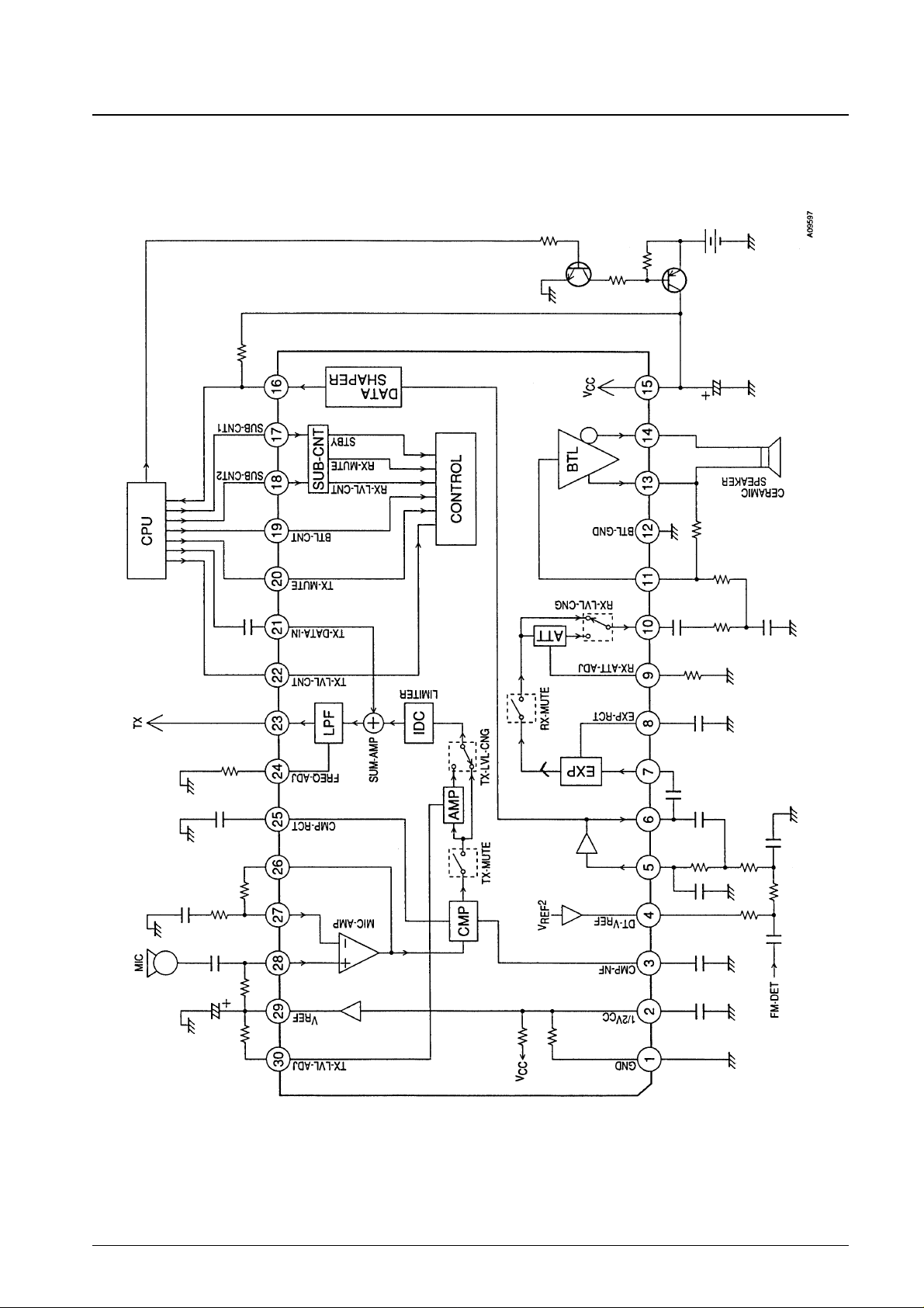
Block Diagram
No. 5776-3/16
LA8638V
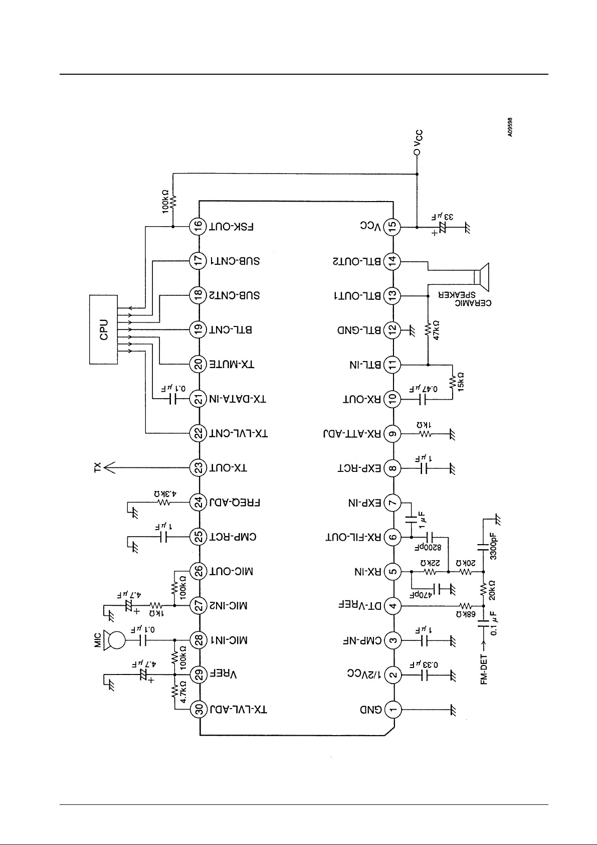
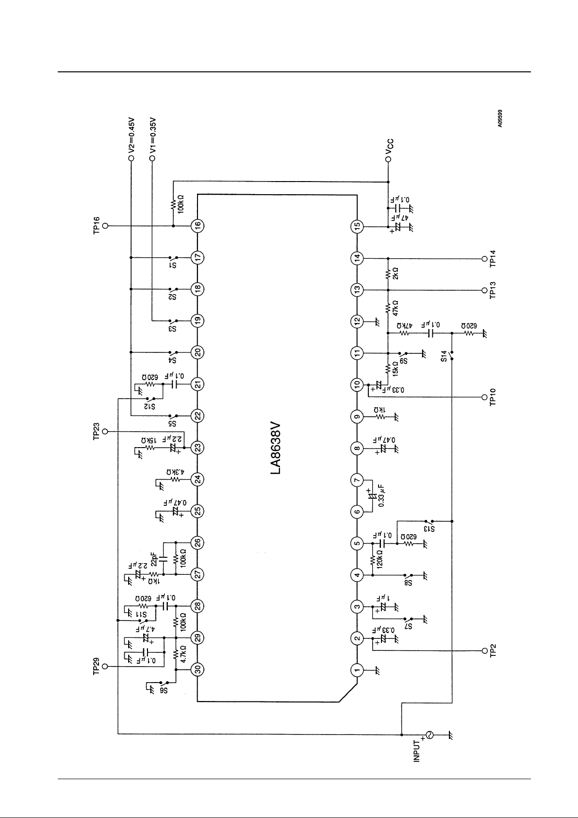
Sample Application Circuit
No. 5776-4/16
LA8638V
Test Circuit
No. 5776-5/16
LA8638V
 Loading...