

Ordering number : EN6075
30499RM (OT) No. 6075-1/17
Overview
The LA8520M is an I/O switching audio signal-processing
IC for use in facsimile units and telephones. It integrates a
crosspoint switch, a BTL power amplifier, an electronic
volume control, a microphone amplifier, and other
functions on a single chip.
Applications
Personal facsimile units and telephones
Functions
• Crosspoint switch (equivalent to an 8 × 8 switch)
• BTL power amplifier
• Electronic volume control
• Serial interface
Features
• Built-in BTL power amplifier (8 to 32 Ω load): VCC=
5 V, RL= 16 Ω, Pomax = 250 mW
• Electronic volume control (BTL power amplifier
system: seven 4-dB steps, receiver amplifier system: two
3-dB steps)
• Low switching noise, low crosstalk characteristics
(crosspoint switch)
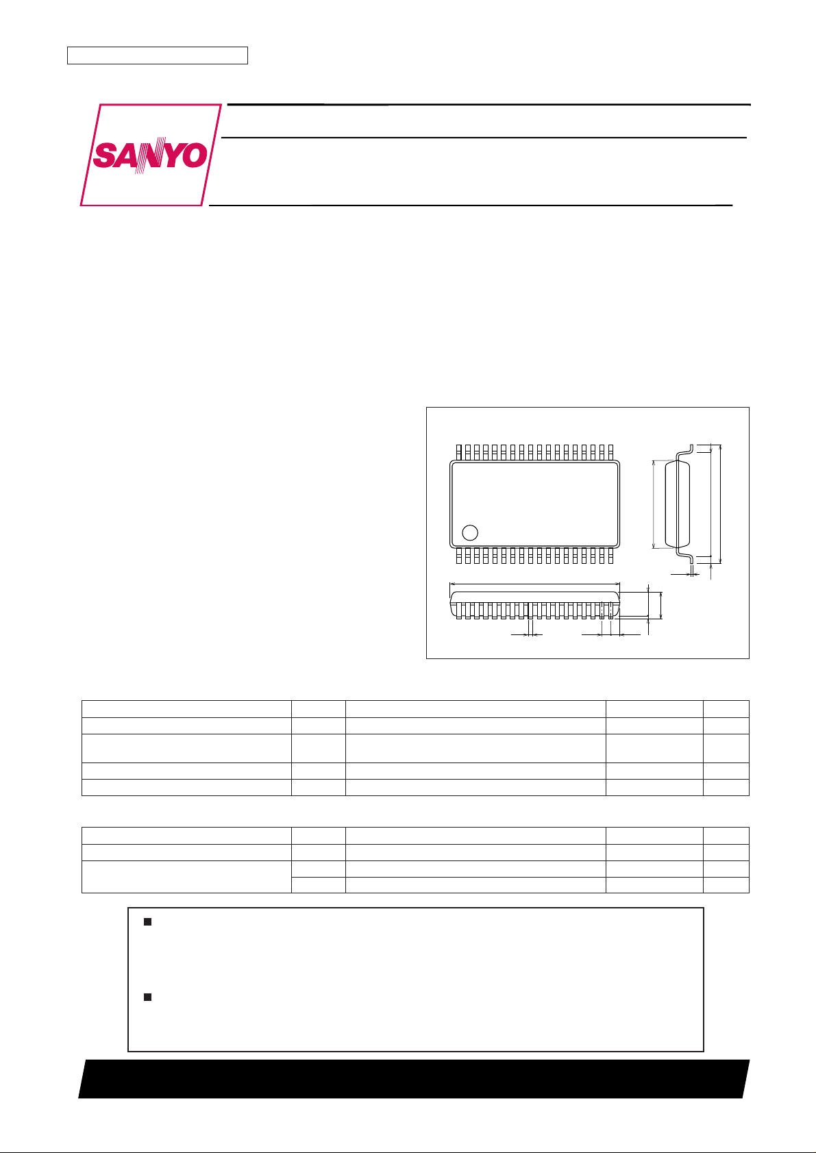
Package Dimensions
unit: mm
3129-MFP36SD
0.25
15.3
1
18
36
19
0.85
0.4
0.8
2.5max
2.25
0.1
7.9
9.2
10.5
0.65
SANYO: MFP36SD
[LA8520M]
LA8520M
SANYO Electric Co.,Ltd. Semiconductor Bussiness Headquarters
TOKYO OFFICE Tokyo Bldg., 1-10, 1 Chome, Ueno, Taito-ku, TOKYO, 110-8534 JAPAN
Audio Signal-Processing IC with I/O Switching
Monolithic Linear IC
Any and all SANYO products described or contained herein do not have specifications that can handle
applications that require extremely high levels of reliability, such as life-support systems, aircraft’s
control systems, or other applications whose failure can be reasonably expected to result in serious
physical and/or material damage. Consult with your SANYO representative nearest you before using
any SANYO products described or contained herein in such applications.
SANYO assumes no responsibility for equipment failures that result from using products at values that
exceed, even momentarily, rated values (such as maximum ratings, operating condition ranges, or other
parameters) listed in products specifications of any and all SANYO products described or contained
herein.
Parameter Symbol Conditions Ratings Unit
Maximum supply voltage V
CC
max 15 V
Allowable power dissipation Pd max
Ta ≤ 70°C
600 mW
(Mounted on a glass-epoxy board: 114.3 × 76.1 ×1.6 mm3)
Operating temperature Topr –20 to +70 °C
Storage temperature Tstg –40 to +150 °C
Specifications
Maximum Ratings at Ta = 25°C
Parameter Symbol Conditions Ratings Unit
Recommended supply voltage V
CC
5V
Allowable operating supply voltage range
V
CCop
4.5 to 7.5 V
V
CCopbtl
4.5 to 9.0 V
Operating Conditions at Ta = 25°C
No. 6075-2/17
LA8520M
Parameter Symbol Conditions
Ratings
Unit
min typ max
Crosspoint switch voltage gain Gsw Vin = –13 dBV –2.5 –0.5 1.5 dB
Crosspoint switch maximum input level Vimax THD = 1.5 % –13 –7 — dBV
Crosspoint switch output noise voltage Nosw 20 to 20 kHz 15 60 µVrms
Microphone amplifier/TR amplifier voltage gain Gmic Vin = –53 dBV 38 40 42 dB
Microphone amplifier/TR output distortion THDmc Vin = –53 dBV — 0.6 1.5 %
Microphone amplifier/TR equivalent input noise
Nimc Rg = 620 Ω, 20 to 20 kHz 2.5 7.5 µVrms
voltage
Microphone amplifier/TR maximum voltage gain Gmax 40 — — dB
Receiver amplifier/OGM amplifier voltage gain Gre Vin = –33 dBV 18 20 22 dB
Receiver amplifier/OGM amplifier output
THDre Vin = –33 dBV 0.4 1.5 %
distortion
Operational amplifier voltage gain Gop Vin = –13 dBV 8 10 12 dB
Operational amplifier output distortion THDop Vin = –13 dBV — 0.4 1.5 %
DR amplifier output level Vodr Vin = –23 dBV, IN(8), OUT(32), sw(10) on –16.1 –13.6 –11.1 dBV
DR amplifier output distortion THDdr Vin = –23 dBV, IN(8), OUT(32), sw(10) on 0.5 1.5 %
Handset amplifier output level Vohd Vin = –16 dBV, IN(9), OUT(34), sw(0B) on –2 +0.5 +3 dBV
Handset amplifier output distortion THDhd Vin = –16 dBV, IN(9), OUT(34), sw(0B) on — 0.55 1.5 %
Handset amplifier attenuator level 1 Att1 address (51) 2.3 3 3.7 dB
Handset amplifier attenuator level 2 Att2 address (52) 3.45 4.15 4.85 dB
Handset amplifier attenuator level 3 Att3 address (53) 5.4 6.1 6.8 dB
Electronic volume control output level Voevr Vin = –20 dBV, IN(9), OUT(28), sw(2D) on –22.9 –20.4 –17.9 dBV
Electronic volume control step size Wevr Vin = –20 dBV, IN(9), OUT(28), sw(2D) on 2.9 3.8 4.6 dB
Electronic volume control output noise voltage Noevr 20 to 20 kHz, OUT(28) — 25 60 µVrms
[BTL Power Amplifier]
Voltage gain Gpwr Vin = –20 dBV, R
L
= 16 Ω 18.2 19.7 21.2 dB
Total harmonic distortion THDpw Vin = –30 dBV, R
L
= 16 Ω — 0.7 1.5 %
Maximum BTL output power Pomax THD = 10 %, R
L
= 16 Ω 250 400 — mW
Ripple rejection ratio SVRR
Rg = 620 Ω, frin = 100 Hz, Vrin = –20 dBV,
40 50 — dB
RL= 16 Ω
Output noise voltage Nopw Rg = 620 Ω, 20 to 20 kHz, R
L
= 16 Ω — 20 60 µVrms
[CPU Interface]
Clock frequency Fck — — 500 kHz
Input signal high level V
H
3 — — V
Input signal low level V
L
— — 1.5 V
[V
REF
and Current Drain]
Internal reference voltage (the pin 10 voltage) Vref 2.1 2.25 2.4 V
Quiescent current 1 Icco1
With the BTL power amplifier on and the
— 21 29 mA
crosspoint switch off
Quiescent current 2 Icco2
With the BTL power amplifier off and the
— 14.5 21 mA
crosspoint switch off
Electrical Characteristics at Ta = 25°C, VCC= 5 V, fin = 1 kHz, RL= 10 kΩ

No. 6075-3/17
LA8520M
Power supply
Block Diagram and Application
8 to 32 Ω
Units (resistance: Ω, capacitance: F)

No. 6075-4/17
LA8520M
Data generator
Test Circuit Diagram
Power
supply
Units (resistance: Ω, capacitance: F)

Serial Data Format
A6 to A0: Setting for the crosspoint switch and control switch address (hexadecimal → binary)
D: Controls the on/off state of the crosspoint switch and control switch.
D = 1: Crosspoint switch on, BTL amplifier on
D = 0: Crosspoint switch off, BTL amplifier off
(The electronic volume control and attenuator can be set to either 0 or 1.)
Other addresses
Address Mode
00 All crosspoint switches off, default settings for the control switches
3F BTL power amplifier on (The default state is off.)
40 Electronic volume control 0 dB ← Default setting
41 Electronic volume control –4 dB
42 Electronic volume control –8 dB
43 Electronic volume control –12 dB
44 Electronic volume control –16 dB
45 Electronic volume control –20 dB
46 Electronic volume control –24 dB
47 Electronic volume control –28 dB
50 Handset amplifier attenuator 0 dB ← Default setting
51 Handset amplifier attenuator –3 dB
52 Handset amplifier attenuator –4 dB
53 Handset amplifier attenuator –6 dB
No. 6075-5/17
LA8520M
Address table
Input - Output LINE HAND RF1 RF2 DOOR AUX EVR OP
RE. — 07 0D 14 — 21 29 2F
TR. 01 — 0E 15 1B 22 — 30
RF1 02 08 38 16 1C 23 2A 31
RF2 03 09 0F 39 1D 24 2B 32
DOOR — 0A 10 17 — 25 2C 33
AUX 04 0B 11 18 1E 26 2D 34
MIC 05 — 12 19 1F 27 — 35
OGM 06 0C 13 1A 20 28 2E 36
OP — — — — — — 37 —
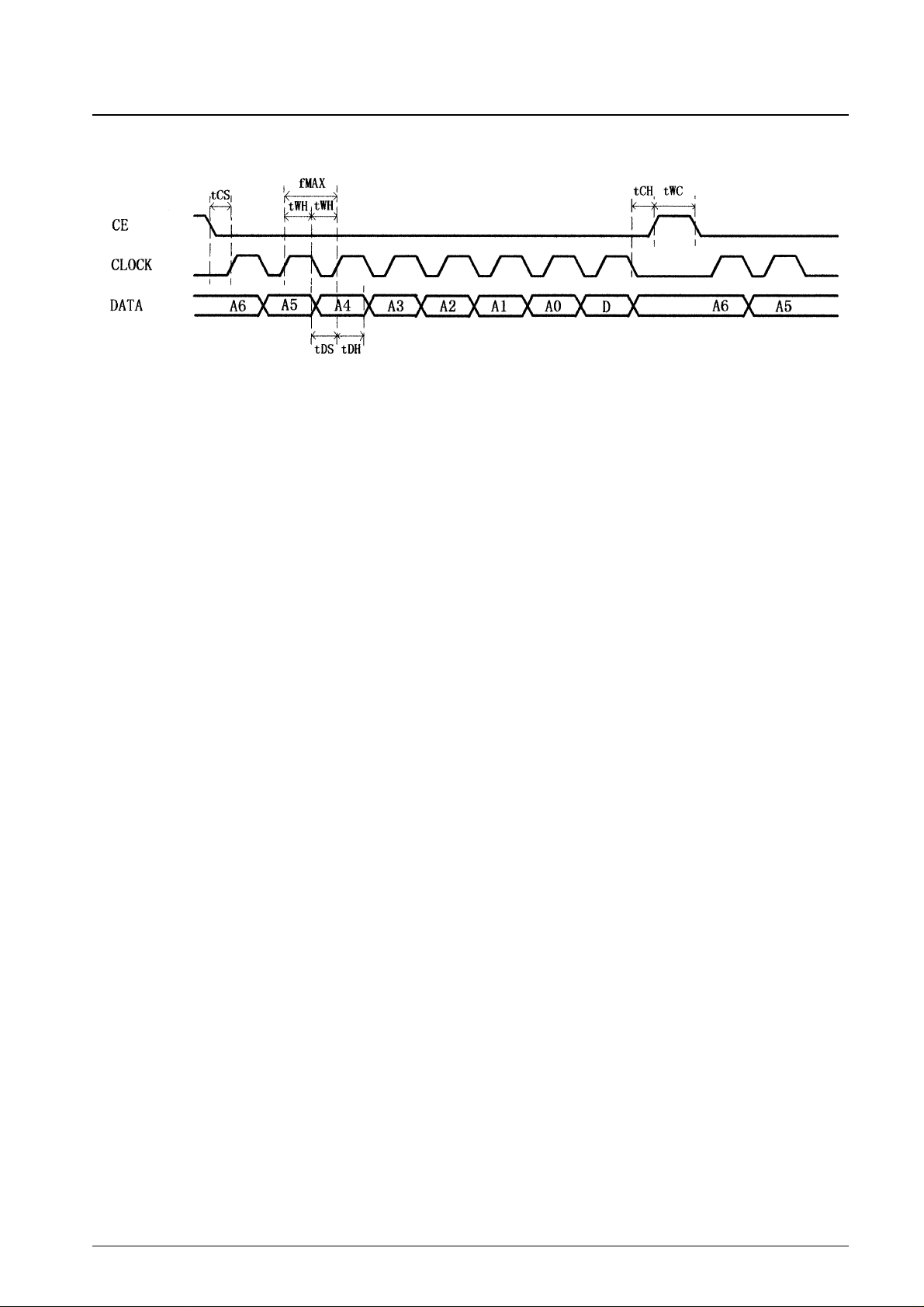
Serial Data Timing
• f
MAX
(Maximum clock frequency) 500 kHz
• tWL(Low-level clock pulse width) At least 1 µs
• tWH(High-level clock pulse width) At least 1 µs
• tCS(Chip enable setup time) At least 1 µs
• tCH(Chip enable hold time) At least 1 µs
• tDS(Data setup time) At least 1 µs
• tDH(Data hold time) At least 1 µs
• tWC(Chip enable pulse time) At least 1 µs
No. 6075-6/17
LA8520M
 Loading...