


Any and all SANYO products described or contained herein do not have specifications that can handle
applications that require extremely high levels of reliability, such as life-support systems, aircraft’s
control systems, or other applications whose failure can be reasonably expected to result in serious
physical and/or material damage. Consult with your SANYO representative nearest you before using
any SANYO products described or contained herein in such applications.
SANYO assumes no responsibility for equipment failures that result from using products at values that
exceed, even momentarily, rated values (such as maximum ratings, operating condition ranges, or other
parameters) listed in products specifications of any and all SANYO products described or contained
herein.
Overview
The LA8519M is a cordless telephone base unit IC that
provides I/O switching, voice signal processing, and other
functions. It integrates, on a single chip, crosspoint switch,
power amplifier, electronic volume and tone control,
microphone amplifier, speech network, and other
functions.
Functions
• Speech network block
— Impedance matching, 2-wire/4-wire converter,
line driver, BN circuit network switching circuit,
transmitter amplifier, BTL receiver amplifier,
DTMF input, key tone input, receiver volume
level switching, and power supply switching
circuit.
• Audio signal-processing block
— Power amplifier, electronic volume and tone
control, preamplifier with ALC, voice level
detection (VOX), beep tone input, ring tone
(OSC) input, ring tone level switching, line
volume level switching, microphone amplifier,
crosspoint switch (10 × 9 point equivalent), and
serial interface.
Features
• Allows switching between two anti-sidetone networks
(near terminal/far terminal) depending on the line
current, and thus achieves excellent sidetone
characteristics over a wide range of line currents.
• Built-in transmitter/receiver amplifier driver power
supply switching circuit allows communication using
extension without power from the telephone network.
• The receiver amplifier supports both ceramic receivers
(BTL) and dynamic receiver (single).
• Built-in power amplifier (load: 8 to 32 Ω): VCC= 5 V,
RL= 8 Ω, Pomax = 200 mW
• The power amplifier signal path includes an electronic
volume control (7 steps of about 3.8 dB each)
• Includes a 10-input/9-output crosspoint switch that
provides mixing functions for easy implementation of
systems that support a diverse range of signal path
switching functions.
Package Dimensions
Unit:mm
3159-QIP64E
Monolithic Linear IC
Ordering number : ENN6471
N3000RM (OT) No. 6471-1/29
SANYO Electric Co.,Ltd. Semiconductor Company
TOKYO OFFICE Tokyo Bldg., 1-10, 1 Chome, Ueno, Taito-ku, TOKYO, 110-8534 JAPAN
I/O Switch/Voice Signal-Processing IC
for Cordless Telephones
LA8519M
14.0
17.2
1.0
1.0
1.6
0.15
0.35
0.1
15.6
0.8
0.8
3.0max
1
16
17
32
33
48
49
64
2.7
14.0
17.2
1.0
1.0
1.6
0.8
SANYO: QIP64E
[LA8519M]

Ratings
Parameter Symbol Conditions
min typ max
unit
[Speech Network Block] at Ta = 25°C, Power supplied: V
CC
= 5 V, fIN= 1 kHz
Line voltage
V
L
1I
L
= 20 mA 3.3 3.8 4.3 V
(20 mA, power supplied/power off)
Line voltage
V
L
2I
L
= 50 mA 4.5 5.2 6.0 V
(50 mA, power supplied/power off)
Line voltage
EV
L
3IL= 120 mA 7.1 8.5 9.9 V
(120 mA, power supplied)
Line voltage
LV3I
L
= 120 mA 7.0 8.4 9.8 V
(120 mA, power off)
Transmitter gain
EGt1 IL= 20 mA, VIN= –55 dBV 42.5 44.5 46.5 dB
(20 mA, power supplied)
Transmitter gain
Gt1 IL= 20 mA, VIN= –55 dBV 42.3 44.3 46.3 dB
(20 mA, power off)
Transmitter gain
Gt2 IL= 120 mA, VIN= –55 dBV 38.3 40.3 42.3 dB
(120 mA, power supplied/power off)
Receiver gain
EGr1 I
L
= 20 mA, VIN= –20 dBV –0.9 1.1 3.1 dB
(20 mA, power supplied)
Receiver gain
EGr2 IL= 120 mA, VIN= –20 dBV –7.4 –5.4 –3.4 dB
(120 mA, power supplied)
Receiver gain
Gr1 IL= 20 mA, VIN= –20 dBV –5.4 –3.4 –1.4 dB
(20 mA, power off)
Receiver gain
Gr2 IL= 120 mA, VIN= –20 dBV –8.7 –6.7 –4.7 dB
(120 mA, power off)
DTMF gain
Gmf1 IL= 20 mA, VIN= –30 dBV 27.7 29.7 31.7 dB
(20 mA, power supplied/power off)
DTMF gain
Gmf2 I
L
= 120 mA, VIN= –30 dBV 23.6 25.6 27.6 dB
(120 mA, power supplied/power off)
KT gain (power supplied) EGkt IL= 20 mA/120 mA, VIN= –40 dBV 10.0 12.0 14.0 dB
KT gain (20 mA, power off) Gkt1 I
L
= 20 mA, VIN= –40 dBV 5.8 7.8 9.8 dB
KT gain
(120 mA, power off)
Gkt2 IL= 120 mA, VIN= –40 dBV 9.0 11.0 13.0 dB
Transmitter dynamic range
DRt1 I
L
= 20 mA, THD = 4% 2.5 5.6 Vp-p
(20 mA, power supplied/power off)
Transmitter dynamic range
DRt2 I
L
= 120 mA, THD = 4% 4.5 7.7 Vp-p
(120 mA, power supplied/power off)
Receiver dynamic range
EDRs I
L
= 20 mA/120 mA, RL= 150 Ω, THD = 10% 0.5 1.5 Vp-p
(power supplied)
Receiver dynamic range
DRs1 RL= 150 Ω, IL= 20 mA, THD = 10% 0.3 0.55 Vp-p
(20 mA, power off)
Receiver dynamic range
DRs2 RL= 150 Ω, IL= 120 mA, THD = 10% 0.5 1.4 Vp-p
(120 mA, power off)
Electrical Characteristics
Continued on next page.
No. 6471-2/29
LA8519M
Specifications
Maximum Ratings at Ta = 25°C
Operating Conditions at Ta = 25°C
Parameter Symbol Conditions Ratings Unit
Maximum supply voltage
V
CC
max 15 V
V
L
max 15 V
Line current I
L
max 130 mA
Allowable power dissipation Pd max Ta ≤ 70°C
(Mounted on a glass epoxy board: 120 × 120 × 1.6 mm3)
1000 mW
Operating temperature Topr –20 to +70 °C
Storage temperature Tstg –40 to +150 °C
Parameter Symbol Conditions Ratings Unit
Recommended supply voltage V
CC
Other than the speech network 5.0 V
Allowable operating supply voltage range
V
CC
op Pin 17 4.5 to 6.5 V
V
CC
oppwr Pin 28 4.5 to 9.5 V

No. 6471-3/29
LA8519M
Continued from preceding page.
Ratings
Parameter Symbol Conditions
min typ max
unit
Receiver BTL dynamic range
EDRb IL= 20 mA/120 mA, RL= 3 kΩ, THD = 10% 5 10 Vp-p
(power supplied)
Receiver BTL dynamic range
DRb1 RL= 3 kΩ, IL= 20 mA, THD = 10% 2 3.4 Vp-p
(20 mA, power off)
Receiver BTL dynamic range
DRb2 RL= 3 kΩ, IL= 120 mA, THD = 10% 5 8.4 Vp-p
(120 mA, power off)
MUTE input high-level voltage
V
IH
IL= 20 mA to 120 mA 0.6 VSP V
(power supplied/power off)
MUTE input low-level voltage
V
IL
IL= 20 mA to 120 mA 0 0.4 V
(power supplied/power off)
Transmitter PADC attenuation
∆Gt IL= 40 mA, pin 34: grounded through 24 Ω 4.0 dB
(power supplied/power off)
Receiver PADC attenuation
∆Gr IL= 40 mA, pin 34: grounded through 24 Ω 6.0 dB
(power supplied/power off)
Internal supply voltage
EV
SP
IL= 20 mA/120 mA 4.75 V
(power supplied)
Internal supply voltage
VSP1IL= 20 mA 1.92 V
(20 mA, power off)
Internal supply voltage
VSP2IL= 120 mA 4.74 V
(120 mA, power off)
Internal reference voltage
ES-V
REFIL
= 20 mA/120 mA 2.26 V
(power supplied)
Internal reference voltage
S-V
REF
1IL= 20 mA 0.79 V
(20 mA, power off)
Internal reference voltage
S-V
REF
2IL= 120 mA 1.92 V
(120 mA, power off)
[Voice Signal-Processing Block] at Ta = 25°C, V
CC
= 5 V, fIN= 1 kHz, RL= 10 kΩ
(Crosspoint switch)
Voltage gain G
SW
VIN= –13 dBV, pin 58 input, pin 2 output –2.5 –0.5 1.5 dB
Maximum input level V
IN
max THD = 1.5% –13.5 –7.5 dBV
Output noise voltage V
NOSW
Rg = 620 Ω, 20 to 20 kHz 7.0 40 µVrms
(Preamplifier: input from the crosspoint switch)
Voltage gain VG
C
VIN= –45 dBV 8.5 10.5 12.5 dB
Total harmonic distortion THD V
IN
= –20 dBV 0.26 1.0 %
ALC saturated output level V
OS
VIN= –20 dBV 93 115 137 mVrms
ALC range ALC
W
From the point the ALC circuit turns on to the point the THD reaches 1%.
15 dB
Output noise voltage V
NO
Rg = 620 Ω, 20 to 20 kHz 65 250 µVrms
(Microphone amplifier)
Voltage gain VGm V
IN
= –40 dBV 27.5 29.5 31.5 dB
Total harmonic distortion THD V
IN
= –40 dBV 0.05 1.0 %
Output noise voltage V
NO
Rg = 620 Ω, 20 to 20 kHz 65 250 µVrms
(Power amplifier)
Voltage gain VGp R
L
= 8 Ω, VIN= –30 dBV 27.5 29.5 31.5 dB
Maximum output power Po R
L
= 8 Ω, THD = 10% 200 275 mW
Total harmonic distortion THD V
IN
= –30 dBV 0.8 1.5 %
Ripple rejection ratio SVRR Rg = 620 Ω, fr = 100 kHz, Vr = –20 dBV 40 50 dB
Output noise voltage V
NO
Rg = 620 Ω, 20 to 20 kHz 35 100 µVrms
(VOX)
Sensitivity 1 low level V
OX
LVIN= –40 dBV, RL= 100 kΩ 0.1 0.3 V
Sensitivity 2 high level V
OX
HVIN= –44 dBV, RL= 100 kΩ 4.8 4.95 V
(Electronic volume control)
Step width Evrw 2.9 3.8 4.7 dB
(Attenuator)
R-ATT attenuation ∆GR 5.4 6.4 7.4 dB
LINE-ATT attenuation ∆GL 4.6 5.6 6.6 dB
OSC-ATT attenuation ∆GO 13.1 14.6 16.1 dB
Continued on next page.

No. 6471-4/29
LA8519M
Continued from preceding page.
Ratings
Parameter Symbol Conditions
min typ max
unit
(V
REF
)
Output voltage V
REF
2.07 2.27 2.47 V
(Serial Control)
Clock frequency Fck 500 kHz
Input signal high level V
H
2.3 V
Input signal low level V
L
1.0 V
(Power Supply Switching)
Pin 17 voltage 1 Vch1 The voltage applied to pin 17 is valid. 3.5 V
Pin 17 voltage 2 Vch2 The voltage supplied from pin 48 is valid. 1.0 V
Quiescent current I
CCO
With the power amplifier on 24 33.5 mA
No. 6471-5/29
LA8519M
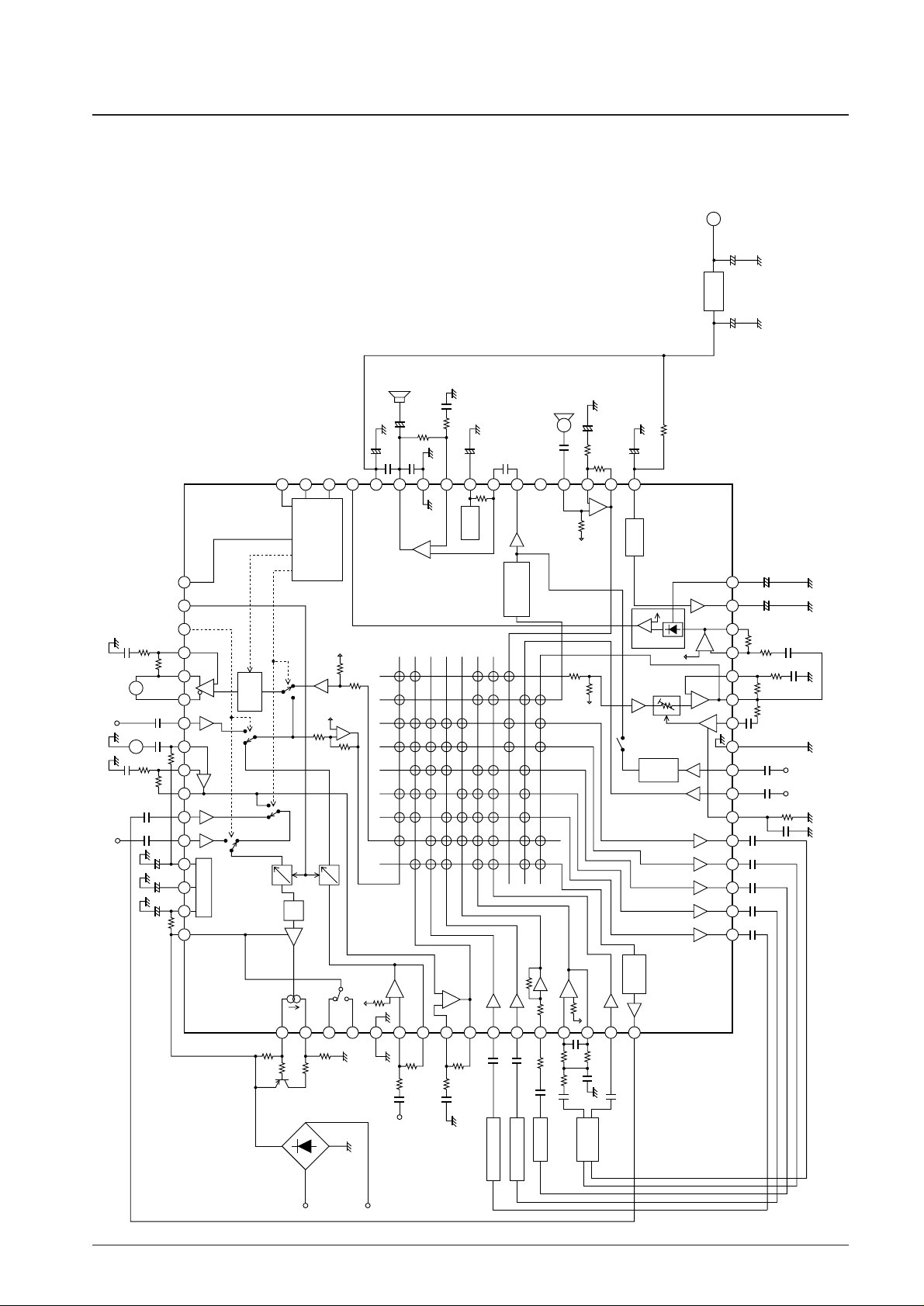
Block Diagram
1234567
0E
8
ALC
VR
SW5
910
OSC-ATT
0/–16DB
–9.5DB
–9.5DB
ALC-OUT
BEEP-IN
OSC-IN
VOX-IN
RESET
(PWR ON RESET)
PAD C
MUTE
MIC
V
REF
VOX-RCT
11
PRE
AMP
12 13 14 15 16
18
19
20
21
22
23
24
25
26
27
28
29
30
31
32
33343536
R
KT
37
3839404142434445464748
49
50
51
52
53
54
55
56
57
58
59
60
61
62
DSP
Compander 1
Compander 2
Door phone
63
64
+ +
+ +
+++
+
+
+
+
+
L-ATT
0/–6DB
P.V
REF
REG
Electronic
volume control
V
CC
EXT.REG
Power supply
5V
PWR MONI
NC
SP
VOX OUT
CE
DATA
CLOCK
PWR-V
CC
PWR-GND
HAND
SW4
SW3
TRANSMIT-AMP
SW2
SW1
GAIN CTL
BN1
BN2
RECEIVER-AMP
Line amplifier
HAND-AMP
RF1
RF2
DOOR
CODEC1
CODEC2
FILTER
EVR
POWER
AMP
MIC
AMP
VOX
CMP
RECT
R-ATT
0/–6DB
LINE-AMP
9.5DB
CPU
INTERFACE
17
16 1D 23 3506
0F 2A 31 3607
29 30 3B
0D 15 1C 22 34 3A05
0C 14 1B 21 33 3904
0B 13 1A 28 2F
0A 12 20 27 2E03
09 19 1F 26 2D02
11 18 1E 25 2C 3801
08 10 17 24 2B 32 37
DTMF
T
1.RF1-OUT
2.RF2-OUT
3.DOOR-OUT
4.CDC1-OUT
5.CDC2-OUT
6.ALC-CNT
7.BEEP-IN
8.OSC-IN
9.GND
10.ALC-IN
11.PRE-OUT
12.PRE-NF
13.VOXA-IN
14.VOXA-OUT
15.V
REF
16.VOX-RCT
17.VCC18.MIC-OUT
19.MIC-NF
20.MIC-IN
21.NC
22.EVR-OUT
23.PWR-IN
24.P-V
REF
25.PWR-NF
26.P-GND
27.PWR-OUT
28.P-VCC29.VOX-OUT
30.CE
31.DATA
32.CLOCK
33.RESET
34.PAD-CNT
35.MUTE
36.RV-NF
37.RV-OUT1
38.RV-OUT2
39.KT-IN
40.TI-IN
41.TI-NF
42.TI-OUT
43.TA-IN
44.DTMF-IN
45.SP-V
REF
46.VSP
47.SP-VCC48.VL
49.TOI
50.TOO
51.BN1
52.BN2
53.SP-GND
54.RI-IN
55.RI-OUT
56.HAND-NF
57.HAND-MONI
58.RF1-IN
59.RF2-IN
60.DOOR-IN
61.FIL-IN
62.FIL-OUT
63.CDC2-IN
64.LINE-OUT
A13120
POWER SUPPLY

No. 6471-6/29
LA8519M
Test Circuit Diagram
12345678910
0.1µF
0.1
µ
F
SW2-2
0.1µF
0.1
µ
F
0.1
µ
F
0.1
µ
F
0.1
µ
F
0.1
µ
F
0.22
µ
F
220
µ
F
1
µ
F
1
µ
F
0.1
µ
F
100
µ
F
0.01
µ
F
0.47
µ
F
10
µ
F
0.1
µ
F
0.1
µ
F
0.1
µ
F
0.1
µ
F
10
µ
F
0.22
µ
F
0.22
µ
F
0.1
µ
F
0.1
µ
F
0.1
µ
F
0.1
µ
F
0.1
µ
F
22µF
47
µ
F
220
µ
F
0.1
µ
F
0.22
µ
F
DRCT-SW
220
µ
F
0.1
µ
F
0.1
µ
F
470
µ
F
100
µ
F
0.22
µ
F
0.1
µ
F
10µF
220k
Ω
10k
Ω
100
k
Ω
VOX-IN-SW
100k
Ω
10k
Ω
3.3k
Ω
2k
Ω
150pF
62k
Ω
8
Ω
(1W)
OUTPUT
VOX-OUT
24k
Ω
620
Ω
51
Ω
7.5K
Ω
8.2K
Ω
5.6K
Ω
8200pF
180pF
6800pF
82
Ω
82
Ω
82
Ω
(1W)
2SA608NP
3.3k
Ω
600
Ω
(10W)
1.3k
Ω
1.8k
Ω
11k
Ω
22k
Ω
39k
Ω
47k
Ω
6.2k
Ω
300
Ω
150
Ω
3k
Ω
0.1
µ
F
20k
Ω
100
k
Ω
100
k
Ω
150
k
Ω
100
k
Ω
51k
Ω
VCC5V
330pF
100k
Ω
620
Ω
100
k
Ω
10k
Ω
11 12 13 14 15 16
18
19
20
21
22
23
24
25
26
27
28
29
30
31
32
33
RESET
PAD-CNT
MUTE
RV-NF
RV-OUT1
RV-OUT2
KT-IN
TI-IN
TI-NF
TI-OUT
TA-IN
DTMF-IN
SP-V
REF
VSP
SP-VOC
VL
343536373839404142434445464748
49 TOI
TOO
BN1
BN2
SP-GND
RI-IN
RI-OUT
HAND-NF
HAND-MONI
LA8519M
RF1-IN
RF2-IN
DOOR-IN
FIL-IN
FILOUT
CDC2-IN
LINE-OUT
50
51
52
53
54
55
56
57
58
59
60
61
62
63
64
+
+
+
+++
+
+
17V
CC
MIC-OUT
INPUT
INPUT
1kHz
620
Ω
1kHz
MIC-NF
MIC-IN
NC
EVR-OUT
PWR-IN
P-V
REF
PWR-NF
P-GND
PWR-OUT
P-V
CC
VOX-OUT
CE
DATA
CLOCK
CE
DATA
CLOCK
Data generator
47K
Ω
A13121
+
RF1-OUT
RF2-OUT
DOOR-OUT
CDC1-OUT
CDC2-OUT
ALC-CNT
BEEP-IN
OSC-IN
GND
ALC-IN
PRE-OUT
PRE-NF
VOXA-IN
VOXA-OUT
V
REF
VOX-RCT
+
SW2-1
SW2-3
SW2-4
SW2-5
SW2-6
SW5-1
SW3-1
SW1-7
SW2-7
SW2-8
SW3-2
SW3-3
SW3-4
RV1RV2
VLSP-IN
PWR-OUT
0.45V
VCNT
IL
+
+
SW4-1
MUTE-SW
BTL-SW
RAD-C-SW
RESET-SW
+
SW4-2
SW4-3
SW4-4
SW1-6
SW1-4
SW1-2
SW1-1
No. 6471-7/29
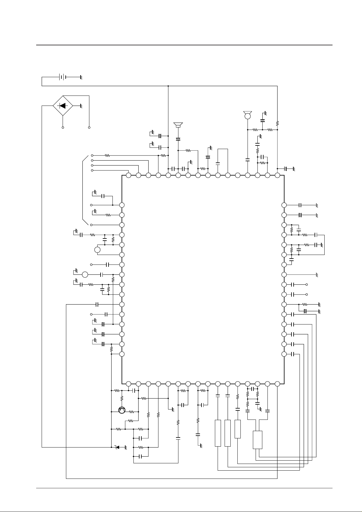
LA8519M
Sample Application Circuit
12345678910
BEEP-IN
0.1
µ
F
0.1
µ
F
0.1
µ
F
0.1
µ
F
0.1
µ
F
0.1
µ
F
0.1
µ
F
0.22
µ
F
220
µ
F
1
µ
F
1
µ
F
0.033
µ
F
220
µ
F
0.01
µ
F
0.47
µ
F
KT-IN
DTMF-IN
0.1
µ
F
0.1
µ
F
0.1
µ
F
0.1
µ
F
0.22
µ
F
0.22
µ
F
0.1
µ
F
0.1
µ
F
0.1
µ
F
0.1
µ
F
0.1
µ
F
100
µ
F
47
µ
F
220
µ
F
0.1
µ
F
0.22
µ
F
220
µ
F
0.1
µ
F
0.1
µ
F
470
µ
F
0.1
µ
F
100
µ
F
0.22
µ
F
0.1
µ
F
330pF
330pF
47µF
220k
Ω
10k
Ω
330pF
3.3k
Ω
2k
Ω
62k
Ω
24k
Ω
620
Ω
51
Ω
7.5K
Ω
8.2K
Ω
8.2
Ω
5.6K
Ω
8200pF
180pF330pF
6800pF
82
Ω
82
Ω
(1W)
2SA608NP
3.3k
Ω
1.3kΩ1.8k
Ω
11k
Ω
22k
Ω
10k
Ω
6.2k
Ω
0.1
µ
F
20k
Ω
51k
Ω
CPU
TIP
VCC5V
LINE
RING
330pF
10k
Ω
OSC-IN
MIC
11 12 13 14 15 16
18
19
20
21
22
23
24
25
26
27
28
29
30
31
32
33
RESET
PAD-CNT
MUTE
RV-NF
RV-OUT1
RV-OUT2
KT-IN
TI-IN
TI-NF
TI-OUT
TA-IN
DTMF-IN
SP-V
REF
VSP
SP-VOC
VL
343536
R
373839404142434445464748
49 TOI
TOO
BN1
BN2
SP-GND
RI-IN
RI-OUT
HAND-NF
HAND-MONI
LA8519M
RF1-IN
RF2-IN
DOOR-IN
FIL-IN
FILOUT
CDC2-IN
LINE-OUT
50
51
52
53
54
55
56
57
58
59
60
61
62
DSP
Compander 1
Compander 2
Door phone
63
64
+
+
+++
+
+
SP
FILTER
17V
CC
MIC-OUT
MIC-NF
MIC-IN
NC
EVR-OUT
PWR-IN
P-V
REF
PWR-NF
P-GND
PWR-OUT
P-V
CC
VOX-OUT
CE
DATA
CLOCK
T
A13122
+
+
+
RF1-OUT
RF2-OUT
DOOR-OUT
CDC1-OUT
CDC2-OUT
ALC-CNT
BEEP-IN
OSC-IN
GND
ALC-IN
PRE-OUT
PRE-NF
VOXA-IN
VOXA-OUT
V
REF
VOX-RCT
100
k
Ω
100
k
Ω
330
pF
100
k
Ω
100
k
Ω
150
k
Ω
100
k
Ω
100
k
Ω
100
k
Ω

Serial Data Format
No. 6471-8/29
LA8519M
Address Table
Output
LINE HAND RF1 RF2 DOOR CDC1 CDC2 EVR PRE
Input
LINE — 08 10 17 — 24 2B 32 37
HAND 01 — 11 18 1E 25 2C — 38
RF1 02 09 — 19 1F 26 2D — —
RF2 03 0A 12 — 20 27 2E — —
DOOR — 0B 13 1A — 28 2F — —
CDC1 04 0C 14 1B 21 — — 33 39
CDC2 05 0D 15 1C 22 — — 34 3A
MIC — — — — — 29 30 — 3B
BEEP 06 0E 16 1D 23 — — 35 —
PRE 07 0F — — — 2A 31 36 —
Address No. Mode
00 Sets all crosspoint and control switches to the off state. *
2
3C ALC control (D = 1: Off, D = 0: On)
3D Transmitter/receiver control (SW1 and SW4 in the block diagram) *
1
3E OSC input (SW5) control (D = 1: On, D = 0: Off)
3F Power amplifier control (D = 1: On, D = 0: Off)
40 Electronic volume control 0 dB ⇒ (Default value)
41 Electronic volume control –4 dB
42 Electronic volume control –8 dB
43 Electronic volume control –12 dB *2
44 Electronic volume control –16 dB
45 Electronic volume control –20 dB
46 Electronic volume control –24 dB
47 Electronic volume control –28 dB
7D Line attenuator (L-ATT) setting (D = 1: –6 dB, D = 0: 0 dB)
7E Receiver attenuator (R-ATT) setting (D = 1: 0 dB, D = 0: –6 dB)
7F Oscillator attenuator (OSC-ATT) setting (D = 1: 0 dB, D = 0: –16 dB)
Other addresses
CE
CLOCK
DATA
A6 A5 A4 A3 A2 A1 A0 D
A6 to A0 ⇒ Sets the address of the crosspoint switch or control switch (hexadecimal ⇒ binary number)
D ⇒ Sets the on/off state of the crosspoint switch or control switch.
(The switch is set to the on state when D is 1, and to the off state when 0.)
* With address 3D set to the on state, SW1 is set to enable the transmitter amplifier output (pin 42) and SW4 is set to enable either the receiver amplifier
output (pin 55) or the KT (pin 39) signal. If a voltage is not supplied to V
CC
(pin 17) (i.e. the power off state), SW1 and SW4 are set to the same states
as when address 3D is set to the on state.
** For addresses 00 and 40 to 47, the data D may be either 0 or 1.
Notes: 1. The receiver attenuator (R-ATT) is set to –6 dB at power on or after a reset (pin 33 set to low, or address 00 accessed).
2. The line attenuator (L-ATT) is set to 0 dB at power on or after a reset (pin 33 set to low, or address 00 accessed).
3. The oscillator attenuator (OSC-ATT) is set to –16 dB at power on or after a reset (pin 33 set to low, or address 00 accessed).
4. The electronic volume control is set to 0 dB at power on or after a reset (pin 33 set to low, or address 00 accessed).
5. Addresses are expressed as hexadecimal numbers.
6. Since the LA8519M includes a power on reset function, all the crosspoint and control switches are reset to their default states when external power
(pin 17: V
CC
) is applied.
7. Switches SW2 and SW3 in the block diagram are controlled by the MUTE pin (pin 35). The table lists the signals enabled by this pin.
MUTE pin (pin 35) SW2 SW3
High/Open
Transmitter (pin 42) and TA-IN (pin 43)
Receiver (pin 55)
Low DTMF pin (pin 44) KT pin (pin 39)
No. 6471-9/29
LA8519M
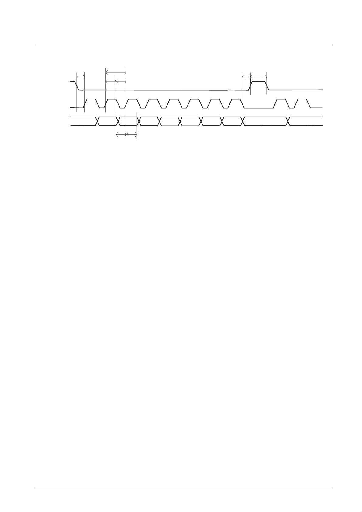
Serial Data Timing
A1
D
CLOCK
DATA
CE
A2
A0
A3
A4
A5
A6
A6
A5
f
MAX
t
WH
t
WH
tDSt
DS
t
CS
tCHt
WC
• f
MAX
(maximum clock frequency) 500 kHz
• t
WL
(clock low-level pulse width) At least 1 µs
• t
WH
(clock high-level pulse width) At least 1 µs
• t
CS
(chip enable setup time) At least 1 µs
• t
CH
(chip enable hold time) At least 1 µs
• t
DS
(data setup time) At least 1 µs
• t
DH
(data hold time) At least 1 µs
• t
WC
(chip enable pulse width) At least 1 µs
Note: The control data must be input at least 400 ms after the supply voltage is applied to the V
CC
pin (pin 17).
 Loading...