

Ordering number: EN5421
Monolithic Linear IC
LA8518NM
Signal Processor for Cordless Telephone Base Sets
Functions
Speech network block
c 2-wire/4-wire conversion
c Line driver
c Transmitting amplifier
c Receiving amplifier (with ATT)
c Power supply switching circuit
c Impedance matching
c DTMF interface
c Key tone interface
c BN circuit network switching circuit
(BN = Balancing Network)
Signal processor block
c Record preamplifier (with ALC)
c Record amplifier
c Power amplifier (V
c Playback equalizer amplifier
c Voice detector (VOX)
c Electronic volume control (4 dB, 7 steps)
Crosspoint switch block
c Crosspoint switches (mixing available)
c CPU interface
=5V,RL=8Ω,PO= 200 mW)
CC
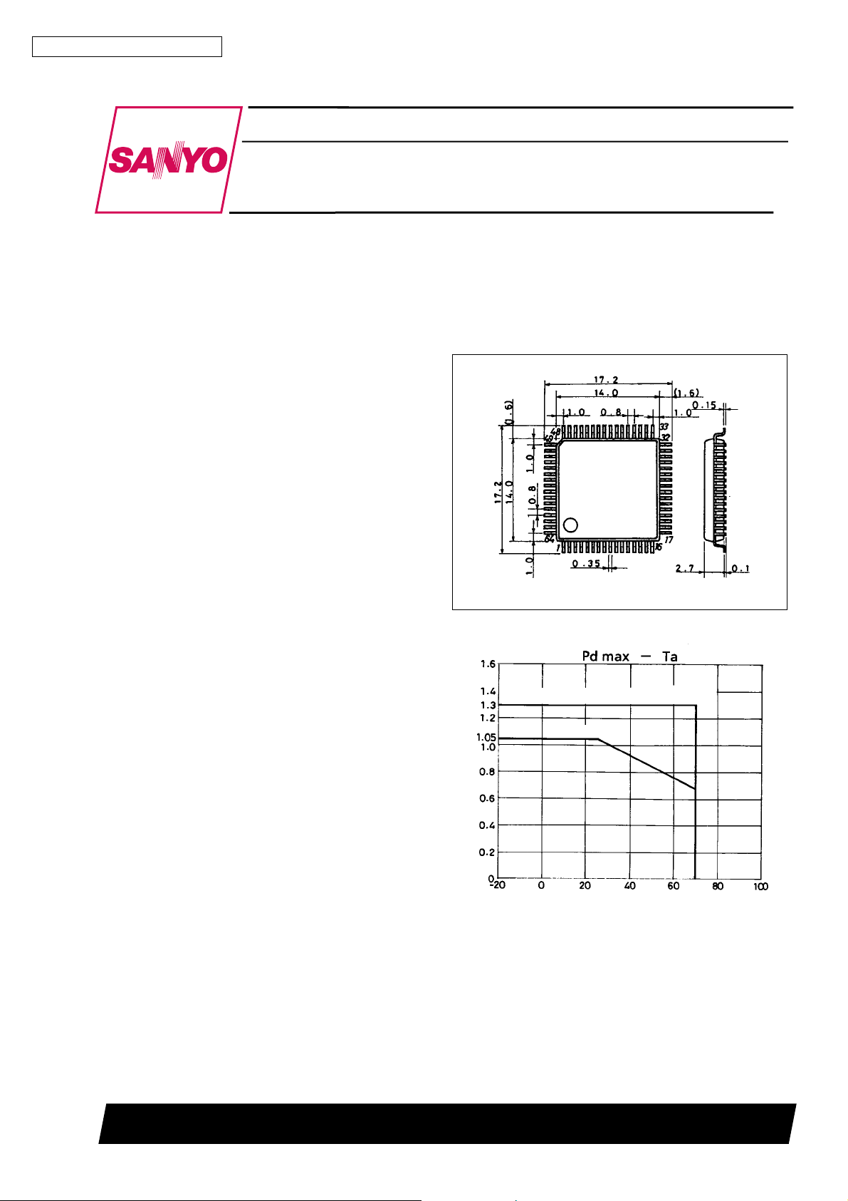
Package Dimensions
unit : mm
3159-QFP64E
[LA8515NM]
SANYO : QIP64E
Features
c Because it is possible to switch the Balancing Network
between two systems, one for the near end and one for the
far end, in accordance with the line current, this IC provides
excellent sidetone characteristics over a wide range of line
currents.
c Receiver amplifier supports ceramic receivers and dynamic
receivers.
c Power amplifier on chip
(V
=5V,RL=8Ω,PO= 200 mW).
CC
c Crosspoint switches allow full mixing, permitting the
implementation of a variety of functions, such as three- or
four-way calls.
c Digital volume control on chip (power system output).
120 × 120 × 1.5 mm3glass epoxy board
Independent IC
Allowable power dissipation, Pd max − W
Ambient temperature, Ta − °C
SANYO Electric Co.,Ltd. Semiconductor Bussiness Headquarters
TOKYO OFFICE Tokyo Bldg., 1-10, 1 Chome, Ueno, Taito-ku, TOKYO, 110 JAPAN
41596HA (II) No.5421-1/31
LA8518NM
Specifications
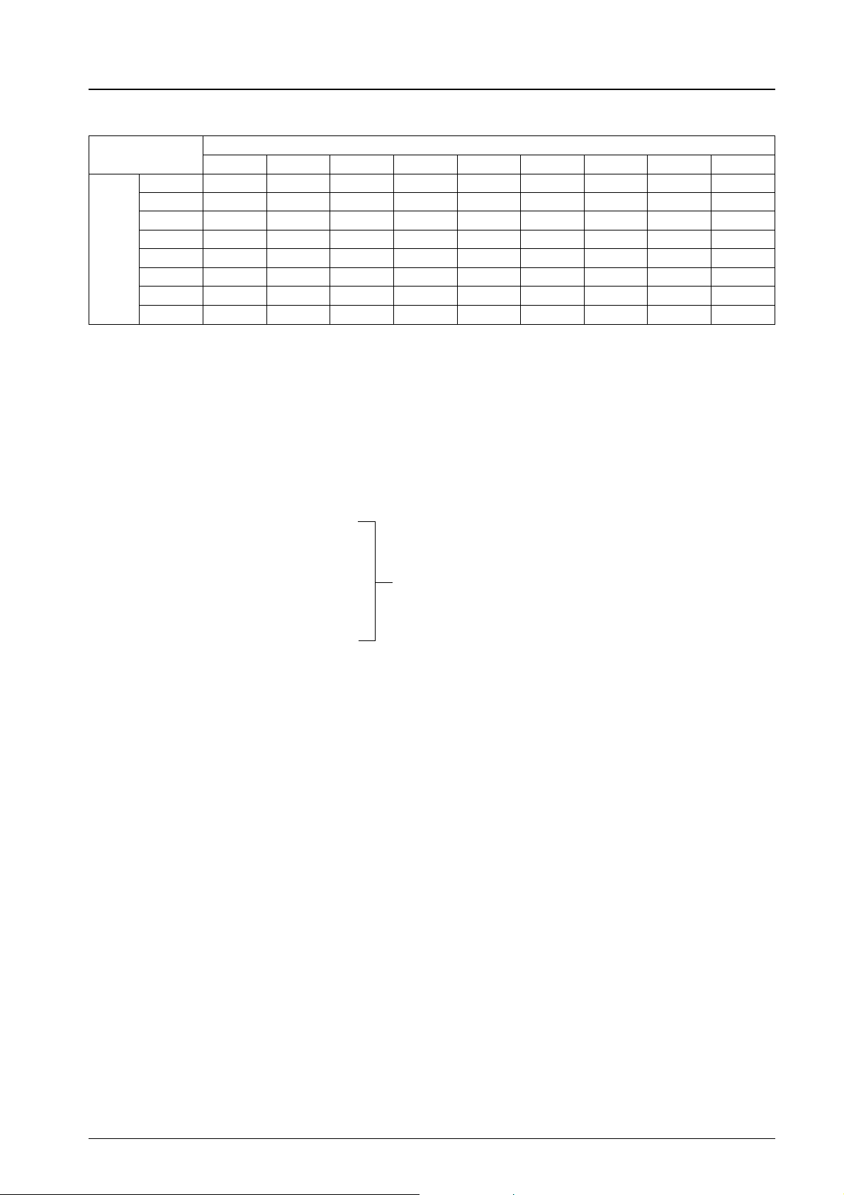
Maximum Ratings at Ta = 25°C
Parameter Symbol Conditions Ratings Unit
V
max Speech network block 15 V
Maximum supply voltage
Line current I
Allowable power dissipation Pd max 1.05 W
Operating temperature Topr –20 to +70 °C
Storage temperature Tstg –40 to +150 °C
Operating Conditions at Ta = 25°C
Parameter Symbol Conditions Ratings Unit
Recommended supply voltage V
Operating supply voltage range V
Operating Characteristics at Ta = 25°C,f=1kHz
Parameter Symbol Conditions min typ max Unit
[Speech Network Block (External power supply operating characteristics)]
Line voltage V
Internal supply voltage V
Transmitting gain G
Receiving gain G
DTMF gain G
KT gain G
Transmitting dynamic range DR
Receiving dynamic range
(Single R
= 150 Ω)
L
Receiving dynamic range
(BTL R
=3kΩ)
L
MUTE high-level input voltage V
MUTE low-level input voltage V
Transmitting PADC attenuation ∆G
Receiving PADC attenuation ∆G
Internal reference voltage V
[Speech Network Block (Operating characteristics when power is off)]
Line voltage V
Internal supply voltage V
DR
DR
L
SP
T
R
MF
KT
DR
SR
IH
IL
REF
L
SP
L
V
max Other than speech network block 10 V
CC
max 130 mA
L
CC
op 4.5 to 7.5 V
CC
Other than speech network block 5 V
IL= 20 mA 3.3 3.9 4.3 V
I
= 50 mA 4.9 5.7 6.5 V
L
I
= 120 mA 7.8 9.3 10.8 V
L
IL= 20 mA 4.5 4.8 5.0 V
I
= 50 mA 4.5 4.8 5.0 V
L
I
= 120 mA 4.5 4.8 5.0 V
L
IL= 20 mA, VIN= –55 dBV 43 45 47 dB
I
= 120 mA, VIN= –55 dBV 39 41 43 dB
L
IL= 20 mA, VIN= –20 dBV –3.0 –1.0 +1.0 dB
I
= 120 mA, VIN= –20 dBV –9.5 –7.5 –5.5 dB
L
IL= 20 mA, VIN= –30 dBV 28 30 32 dB
I
= 120 mA, VIN= –30 dBV 24 26 28 dB
L
IL= 20 mA, VIN= –40 dBV 9 11 13 dB
I
= 120 mA, VIN= –40 dBV 9 11 13 dB
L
IL= 20 mA, THD = 4% 2.5 Vp-p
T
I
= 120 mA, THD = 4% 4.5 Vp-p
L
IL= 20 mA, THD = 10% 0.5 Vp-p
I
= 120 mA, THD = 10% 0.5 Vp-p
L
IL= 20 mA, THD = 10% 5 Vp-p
I
= 120 mA, THD = 10% 5 Vp-p
L
IL= 20 mA to 120 mA
0.6VSP
IL= 20 mA to 120 mA 0 0.4 V
IL= 30 mA, ground at 24 kΩ 3.6 dB
T
IL= 30 mA, ground at 24 kΩ 6.5 dB
R
IL= 20 mA 2.3 V
I
= 50 mA 2.3 V
L
I
= 120 mA 2.3 V
L
IL= 20 mA 3.3 3.8 4.3 V
I
= 50 mA 4.8 5.4 6.2 V
L
I
= 120 mA 7.2 8.7 10.2 V
L
IL= 20 mA 1.7 1.9 2.1 V
I
= 50 mA 2.5 2.8 3.1 V
L
I
= 120 mA 4.55 4.85 5.15 V
L
Continued on next page.
V
No.5421-2/31
Continued from preceding page.
Parameter Symbol Conditions min typ max Unit
Transmitting gain G
Receiving gain G
DTMF gain G
KT gain G
Transmitting dynamic range DR
Receiving dynamic range
(Single R
Receiving dynamic range
(BTL R
MUTE high-level input voltage V
MUTE low-level input voltage V
Transmitting PADC attenuation ∆G
Receiving PADC attenuation ∆G
Internal reference voltage V
= 150 Ω)
L
=3kΩ)
L
DR
DR
T
R
MF
KT
DR
SR
IH
IL
REF
LA8518NM
IL= 20 mA, VIN= –55 dBV 42 44 46 dB
I
= 120 mA, VIN= –55 dBV 39 41 43 dB
L
IL= 20 mA, VIN= –20 dBV –4.5 −2.5 –0.5 dB
I
= 120 mA, VIN= –20 dBV –9 –7 –5 dB
L
IL= 20 mA, VIN= –30 dBV 27 29 31 dB
I
= 120 mA, VIN= –30 dBV 24 26 28 dB
L
IL= 20 mA, VIN= –40 dBV 6.7 8.7 10.7 dB
I
= 120 mA, VIN= –40 dBV 9 11 13 dB
L
IL= 20 mA, THD = 4 % 2.5 Vp-p
T
I
= 120 mA, THD = 4 % 4.5 Vp-p
L
IL= 20 mA, THD = 10% 0.3 Vp-p
I
= 120 mA, THD = 10% 0.5 Vp-p
L
IL= 20 mA, THD = 10% 2 Vp-p
I
= 120 mA, THD = 10% 6 Vp-p
L
IL= 20 mA to 120 mA
IL= 20 mA to 120 mA 0 0.4 V
IL= 30 mA, ground at 24 kΩ 3.7 dB
T
IL= 30 mA, ground at 24 kΩ 6.3 dB
R
IL= 20 mA 0.65 V
I
= 50 mA 1.0 V
L
I
= 120 mA 1.7 V
L
0.6VSP
V
Operating Characteristics at Ta = 25°C,f=1kHz
Parameter Symbol Conditions min typ max Unit
[Audio Signal Processing Block]
PRE AMP Input from crosspoint switch
Voltage gain VG
Total harmonic distortion THD –20 dBV input 0.4 1.0 %
ALC saturation output level V
OS
ALC range ALCW From when ALC is on until THD is 1% 15 dB
Equivalent input noise voltage V
NI
PB AMP
Voltage gain VG
Total harmonic distortion THD –60 dBV input 0.5 1.5 %
Equivalent input noise voltage V
NI
OGM AMP
Voltage gain VG
Total harmonic distortion THD –20 dBV input 0.1 1.0 %
REC AMP
Voltage gain VG
Output bias voltage
V
(Voltage at pin 21)
Total harmonic distortion THD 0.8 1.5 %
MIC AMP
Voltage gain VG
Total harmonic distortion THD –40 dBV input 0.1 1.0 %
Equivalent input noise voltage V
POWER AMP R
=8Ω
L
NI
Voltage gain VG
Output voltage P
Total harmonic distortion THD –30 dBV input 0.6 1.5 %
Input resistance R
IN
Ripple rejection ratio SVRR Rg = 0, fr = 100 Hz, Vr = –20 dBV 40 dB
Output noise voltage V
NO
–45 dBV input 6 8 10 dB
C
–20 dBV input 90 110 130 mVrms
Input AC-shorted, 20 to 20 kHz 5.0 10 µVrms
–60 dBV input 46.5 48.5 50.5 dB
E
Pin AC-shorted, 20 to 20 kHz 5.0 10 µVrms
–20 dBV input 7 9 11 dB
G
Pin 20 ZAC= 8.1 kΩ, between pins 25 and 21 4 6 8 dB
R
Pin 20 ZDC=15kΩ,
B
pin 21 load = 8.2 kΩ
–40 dBV input 27 29 31 dB
M
0.8 1.0 1.2 V
Pin 33 AC-shorted, 20 to 20 kHz 2.0 5 µVrms
–30 dBV input 28 30 32 dB
P
THD = 10% 200 250 mW
O
15 kΩ
Pin 42 AC-shorted, 20 to 20 kHz 0.04 0.1 µVrms
Continued on next page.
No.5421-3/31
Continued from preceding page.
Parameter Symbol Conditions min typ max Unit
VOX
Sensitivity 1 V
Sensitivity 2 V
Electronic volume control
Step width E
VREF
Output voltage V
Control
Clock frequency F
High-level input signal V
Low-level input signal V
Power supply switch
Pin 31 voltage 1 V
Pin 31 voltage 2 V
Quiescent current I
OXL
OXH
VRW
REF
CK
H
L
CH1
CH2
CCO
LA8518NM
–24 dBV input 0.3 V
–27 dBV input 4.8 V
3.8 dB
2.1 2.3 2.5 V
500 kHz
3V
1.5 V
The voltage applied to pin 31 is effective 3.5 V
The voltage supplied from pin 64 is effective 1.2 V
Power amplifier on 19 26 35 mA
No.5421-4/31
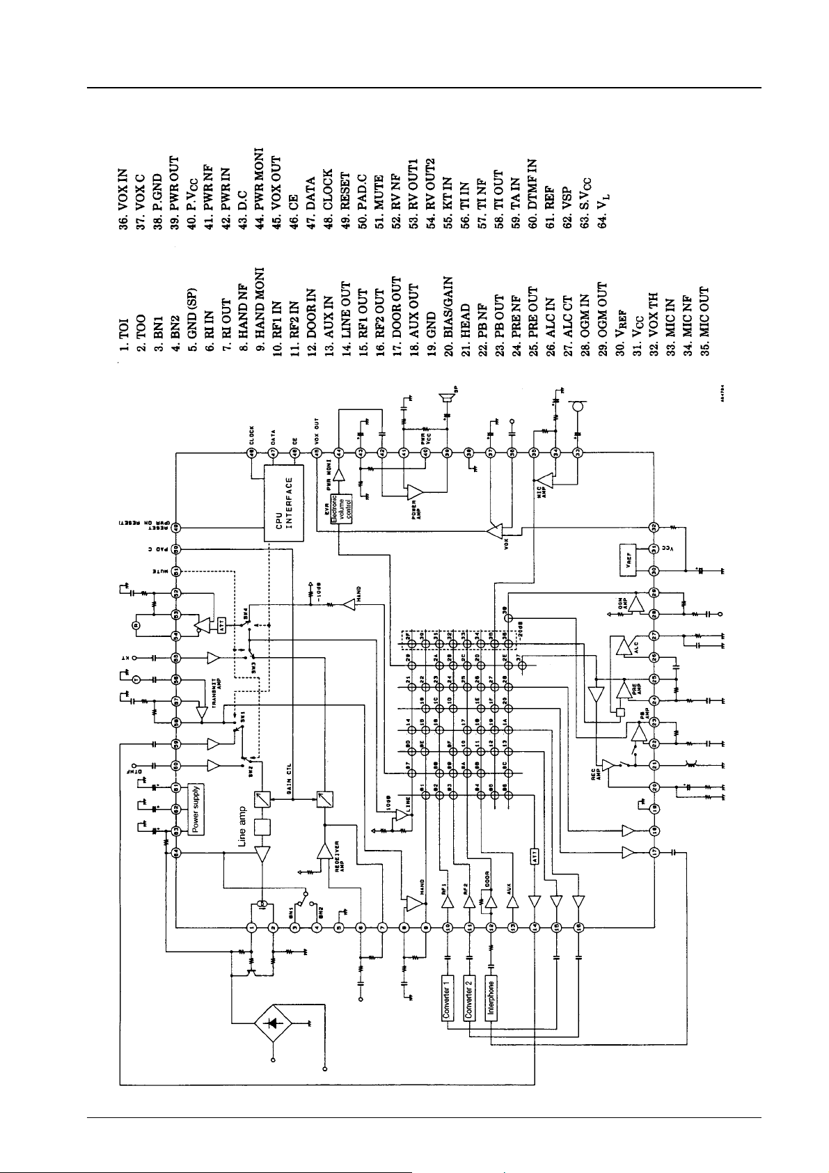
Block Diagram
LA8518NM
No.5421-5/31
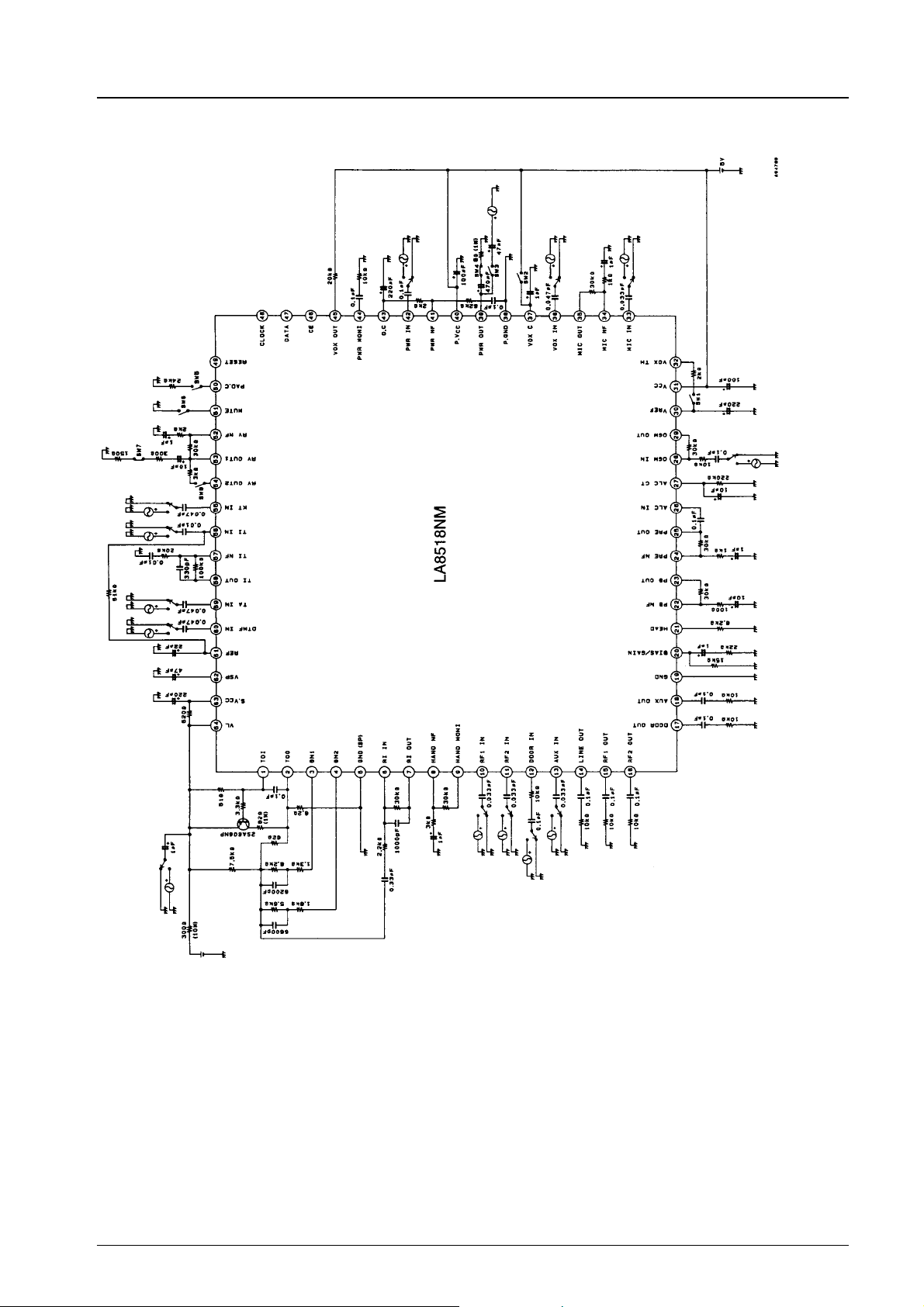
Test Circuit Diagram
LA8518NM
No.5421-6/31
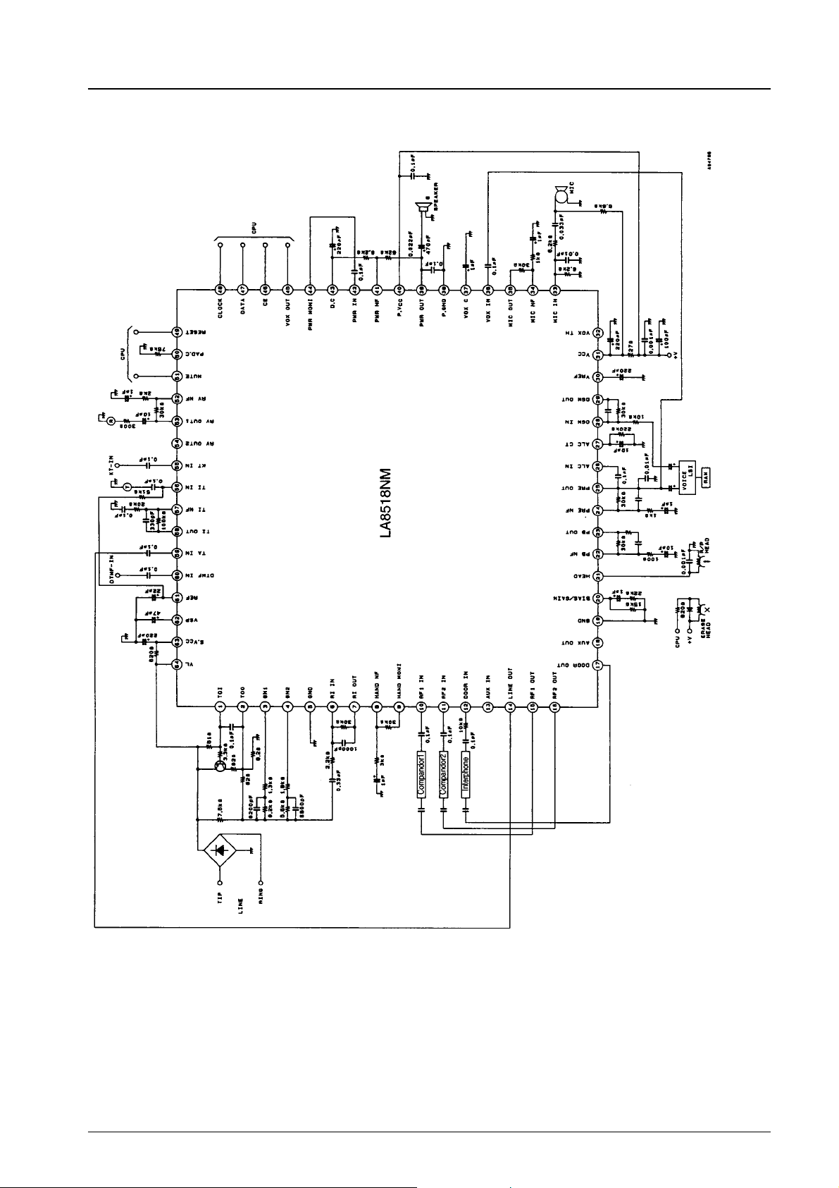
Sample Application Circuit
LA8518NM
No.5421-7/31
LA8518NM
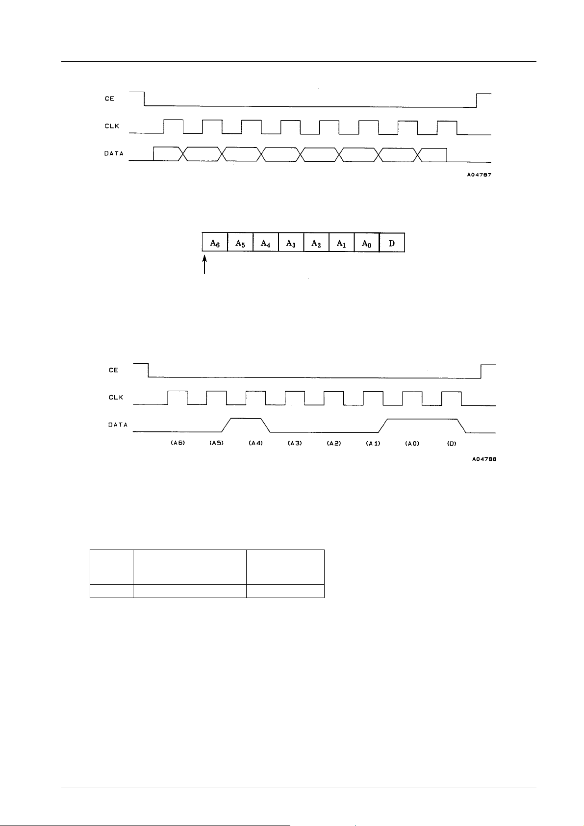
— Serial control data format —
c Serial data content
First bit
A0 to A6 → Specify the address of a crosspoint switch and a control switch.
D → Turns the crosspoint switch on and off and controls the control switch.
(WhenD=1,theswitch is on; whenD=0,theswitch is off.)
c Example: Turning address 11 (AUX input, RF1 output) on
The address table is shown on the following page:
Note 1: Because there is a power-on reset function, all crosspoint switches and control switches are reset when the external power
supply (V
at pin 31) is turned on.
CC
Note 2: SW2 and SW3 in the block diagram are controlled by the MUTE pin (pin 51); the signals that are enabled are shown
below.
MUTE pin SW2 SW3
H
L DTMF (Pin 60) KT (Pin 55)
Transmitting (Pin 58)
TAIN (Pin 59)
Receiving (Pin 7)
No.5421-8/31
LA8518NM
— Address chart —
LINE HAND RF1 RF2 DOOR AUX MIC OGM PRE
LINE — 01 02 03 — 04 05 06 —
HAND 07 — 08 09 0A 0B — 0C —
RF1 0D 0E — 0F 10 11 12 13 —
Output
Other Control Switches
RF2 14 15 16 — 17 18 19 1A —
DOOR — 1B 1C 1D — 1E 1F 20 —
AUX 21 22 23 24 25 26 27 28 —
PWR 29 — 2A 2B 2C 2D — 2E 37
PRE 2F 30 31 32 33 34 35 36 —
00 All crosspoint switches and control switches off *2
38 Mixing switch for PB amplifier-OGM amplifier on
39 Transmitting/receiving CTL (SW1 and SW2 in the block diagram) *1
3A Receiver amplifier ATT Set to 0 dB
3B Line amplifier ATT Set to –6 dB
3C ALC on
3D PB amplifier on
3E REC amplifier on
3F Power amplifier on
40 Electronic volume control 0 dB
41 Electronic volume control –4dB
42 Electronic volume control –8dB
43 Electronic volume control –12dB
44 Electronic volume control –16dB
*2
45 Electronic volume control –20dB
46 Electronic volume control –24dB
47 Electronic volume control –28dB
Input
*1: When address 39 is on, SW1 enables the transmitting amplifier output (pin 58) signal, and SW4 enables the receiving
amplifier output (pin 7) or KT (pin 55) signal. If voltage is not supplied to pin 31 (V
) (power is off), the status of SW1
CC
and SW4 is the same as address 39 is in on state.
*2: When setting address 00 and 40 to 47, ‘‘D’’ data may be either ‘‘0’’ or ‘‘1’’.
Note 1: The receiver amplifier ATT is set to −6 dB when power is first applied, when a reset is performed, and when all of the
switches are off.
Note 2: The line amplifier ATT is set to 0 dB when power is first applied, when a reset is performed, and when all of the switches
are off.
Note 3: The electronic volume control is set to 0 dB when power is first applied, when a reset is performed, and when all of the
switches are off.
Note 4: The addresses are given in hexadecimal notation.
No.5421-9/31
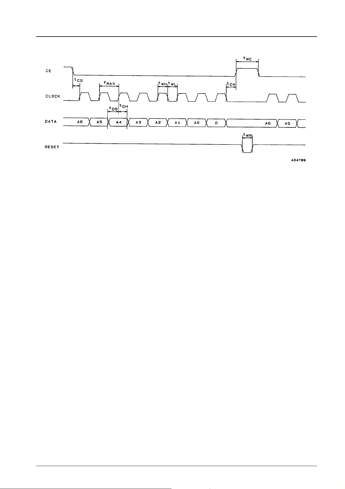
Input Port Timing
LA8518NM
c f
c f
c f
c t
c t
c t
c t
c t
c t
MAX
WL
WH
CS
CH
DS
DH
WC
WR
(Maximum clock frequency) 500 kHz
(Clock pulse width ‘‘L’’) 1µs or longer
(Clock pulse width ‘‘H’’) 1µs or longer
(Chip enable setup time) 1µs or longer
(Chip enable hold time) 1µs or longer
(Data setup time) 1µs or longer
(Data hold time) 1µs or longer
(Chip enable pulse width) 1µs or longer
(Reset pulse width) 1µs or longer
Note: The control data must input 400 ms or longer after the supply voltage is applied to V
CC
(pin 31).
No.5421-10/31
 Loading...