

Page 1
Ordering number : ENN2740B
D2599TH (OT)/N1892TH/7110TS/6028MO, TS No. 2740-1/6
1
10
20
11
0.5
3.25
3.3
3.9max
24.2
0.67
2.54
1.2
0.25
7.62
6.4
SANYO: DIP20
[LA7955]
LA7955
SANYO Electric Co.,Ltd. Semiconductor Company
TOKYO OFFICE Tokyo Bldg., 1-10, 1 Chome, Ueno, Taito-ku, TOKYO, 110-8534 JAPAN
Video Switch for TV / VCR Use
Monolithic Linear IC
Any and all SANYO products described or contained herein do not have specifications that can handle
applications that require extremely high levels of reliability, such as life-support systems, aircraft’s
control systems, or other applications whose failure can be reasonably expected to result in serious
physical and/or material damage. Consult with your SANYO representative nearest you before using
any SANYO products described or contained herein in such applications.
SANYO assumes no responsibility for equipment failures that result from using products at values that
exceed, even momentarily, rated values (such as maximum ratings, operating condition ranges, or other
parameters) listed in products specifications of any and all SANYO products described or contained
herein.
Overview
The LA7955 Video Switch IC is used to switch the video
and audio signals of TVs, VCRs and similar equipment.
Separate pin layouts for the video and audio systems
facilitate board design. Tow signals can be selected from
the three input signals in a symmetrical arrangement
using a control signal. Law impedance lines (VCC, GND
and control input) between the input and output pins
minimize crosstalk caused by the high frequency of the
video section. The LA7955 operates on a 12V power
supply and is available in 20-pin plastic slim DIPs.
Functions
• Video applications : 3 inputs, 2 outputs
• Audio applications : 3 inputs, 2 outputs × 2 (L, R)
channels
• Built-in muting circuits for 2 left and right audio output
channels
Features
• Separate video and audio pin layouts
• Built-in 6dB video amps
• Wideband characteristics
• Minimal video and audio crosstalk
• 12V power supply
• 20-pin plastic slim DIP
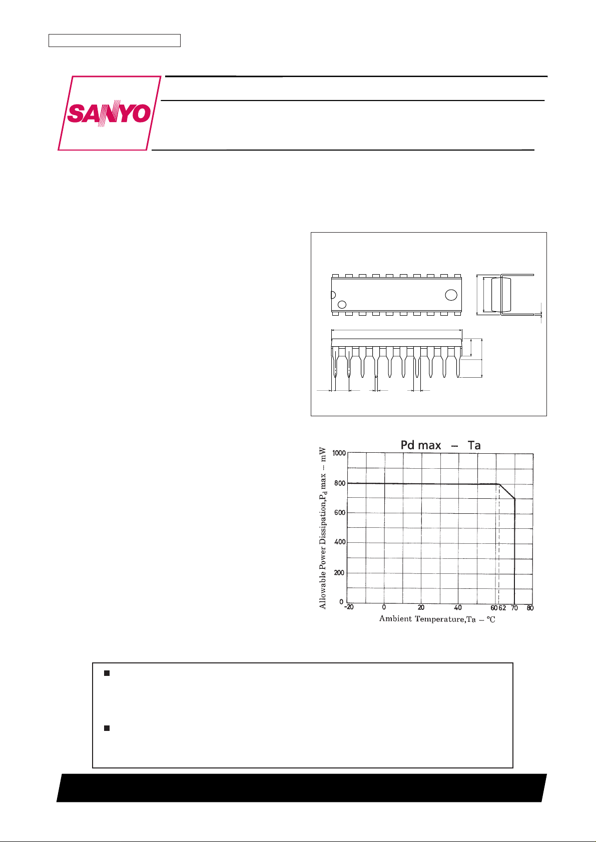
Package Dimensions
unit : mm
3021B-DIP20
Page 2
LA7955
No. 2740-2/6
Parameter Symbol Conditions Ratings Unit
Maximum Supply Voltage V
6
max 14.4 V
V
4
max
Maximum Control Signal Voltage V
8
max 14.4 V
V
10
max
Allowable Power Dissipation Pd max Ta ≤ 70°C 700 mW
Operating Temperature Topr –20 to +70 °C
Storage Temperature Tstg –55 to +125 °C
Specifications
Maximum Ratings at Ta = 25°C
Parameter Symbol Conditions Ratings Unit
Recommended Supply Voltage V
CC
12 V
Operating Supply Voltage Range
VCCop 8 to 13.2 Vs
Operating Conditions at Ta = 25°C
Operating Characteristics at Ta = 25°C, VCC= 12V
Parameter Symbol Conditions
Ratings
Unit
min typ max
Quiescent Current I
CC
35 43 57 mA
Video Input Bias Voltage V
1
, V3, V
7
4.4 4.7 5.0 V
Video Output Bias Voltage V
5
, V
9
6.2 6.8 7.4 V
Video Input Impedance Z
1
, Z3, Z7f = 1 kHz 15 21 27 kΩ
Video Output Impedance Z
5
, Z9f = 1 kHz 42 Ω
Video Voltage Gain G
VV
Vin = 1 Vp-p (sine wave), f = 0.1 MHz 5.6 6.1 6.6 dB
Video Frequency Bandwidth BW
V
Vin = 0.7 Vp-p (sine wave), –3 dB band for 0.1 MHz
10 MHz
Output Noise Voltage Vn
V
Rg = 75 Ω, 10 MHz band
0.3 1.0 mVrms
Video Crosstalk (between inputs 1 and 2) CT
V1
Rg = 75 Ω,
f = 3.58 MHz 45 50 dB
Video Crosstalk (between inputs 1/2 and 3) CT
V2
Rg = 75 Ω,
f = 3.58 MHz 45 50 dB
Video Output Hum Rejection HR
V
f = 50 Hz
, Rg = 75 Ω
18 23 dB
V
12
, V13,
Audio Input Bias Voltage V
14
, V17, 4.5 5.1 5.7 V
V
18
, V
19
Audio Output Bias Voltage
V
11
, V15,
3.2 3.8 4.4 V
V
18
, V
20
Audio Input Impedance (inputs 1 and 2)
Z
12
, Z13,
f = 1 kHz 47 68 88 kΩ
Z
15
, Z
19
Audio Input Impedance (input 3) Z14, Z17f = 1 kHz 51 74 95 kΩ
Audio Output Impedance
Z
11
, Z15,
75 Ω
Z
16
, Z
20
Audio Voltage Gain G
VA
f = 1 kHz, Vin = 500 mVrms –0.5 –0.02 +0.5 dB
Audio Frequency Bandwidth BW
A
–1 dB band (Vin = 500 mVrms) for f = 1 kHz gain
100 kHz
Total Harmonic Distortion THD f = 1 kHz, Vin = 500 mVrms 0.03 0.2 %
Output Noise Voltage Vn
A
Rg = 600 Ω, 20 Hz to 20 kHz bandwidth 10 50 µVrms
Audio Crosstalk (between inputs 1 and 2) CT
A1
Rg = less than 4.7 kΩ, f = 1 kHz (Vin = 500 mVrms)
75 90 dB
Audio Crosstalk (between inputs 1/2 and 3) CT
A2
Rg = less than 4.7 kΩ, f = 1 kHz (Vin = 500 mVrms)
75 90 dB
Audio Crosstalk (between L and R channels) CT
AS
Rg = 4.7 kΩ, f = 1 kHz (Vin = 500 mVrms) 72 82 dB
Mute Noise V
OAM
f = 1 kHz, Vin = 500 mVrms 0.02 0.1 mVrms
Audio Hum Rejection 1 HR1 Input Rg = 4.7 kΩ 40 46 dB
Audio Hum Rejection 2 HR2 Input open 28 39 dB
Switching Control Signal Input High Threshold Voltage
V
4TH
, V
8TH
1.1 1.4 1.7 V
Switching Control Signal Input Leak Current I
4L
, I
8L
–3 µA
Mute Input High Threshold Voltage
V
10TH
1.1 1.4 1.7 V
Mute Input Leak Current I
10L
–3 µA
Note: The current flowing to the IC is positive and current from the IC is negative.
Page 3

LA7955
No. 2740-3/6
Equivalent Circuit Block Diagram
Switching Truth Table
Pin Assignments
Top view
Page 4

LA7955
No. 2740-4/6
Sample Application Circuit
Circuit and Operational Description
1. Video Input circuit
The video input circuit shown in the figure on the right has an input impedance of
approximately 20 kΩ. The input bias voltage is determined by the bias at point
(A), however, the voltage at this point fluctuates according to VCC.
2. Audio input circuit
The audio input circuit is shown in the figure on the right. The impedance of audio
inputs 1 and 2 (Pins 12, 13,18, and 19) is approximately 65 kΩ, and that of audio
input 3 (Pins 14 and 17), approximately 71 kΩ. Although the input bias voltage is
determined by the bias at point (B), the voltage at point (B) is supplied from a lownoise Zener diode voltage regulator circuit and is not dependent on VCC.
3. Control signal input circuit
The circuit at input pins for the switching and muting circuits are shown in the
figure on the right. The threshold voltage is approximately 1.4 V.
Page 5

LA7955
No. 2740-5/6
4. Video Output Circuit
The video output is emitter follower output.
5. Audio output circuit
The audio output is emitter follower output.
6. Video switch operation
SW (A) is switched by the voltage of switching control input signal 1 (Pin 4), and SW (B), by the voltage of
Switching control input signal 2 (Pin 8). In addition, there are amplifiers (with 75 Ω terminating output pins) with a
gain of 6 dB at the pre-output stages of Pins 5 and 9. However, an external buffer is required when shorted with a 75
Ω resistor.
7. Audio switch operation
SW (A) is switched by the voltage of switching control input signal 1 (Pin 4), and SW (B), by the voltage of switching
control input signal 2 (Pin 8). Setting the must input voltage (Pin 10) to H turns the muting switch ON and cutting
output 2.
Two pairs of audio switches are built in, allowing use in equipment designs for multiplex broadcast systems.
Page 6

LA7955
PS No. 2740-6/6
• Application Example 1 (TV with two video inputs)
This catalog provides information as of December, 1999. Specifications and information herein are
subject to change without notice.
Specifications of any and all SANYO products described or contained herein stipulate the performance,
characteristics, and functions of the described products in the independent state, and are not guarantees
of the performance, characteristics, and functions of the described products as mounted in the customer’s
products or equipment. To verify symptoms and states that cannot be evaluated in an independent device,
the customer should always evaluate and test devices mounted in the customer’s products or equipment.
SANYO Electric Co., Ltd. strives to supply high-quality high-reliability products. However, any and all
semiconductor products fail with some probability. It is possible that these probabilistic failures could
give rise to accidents or events that could endanger human lives, that could give rise to smoke or fire,
or that could cause damage to other property. When designing equipment, adopt safety measures so
that these kinds of accidents or events cannot occur. Such measures include but are not limited to protective
circuits and error prevention circuits for safe design, redundant design, and structural design.
In the event that any or all SANYO products (including technical data, services) described or contained
herein are controlled under any of applicable local export control laws and regulations, such products must
not be exported without obtaining the export license from the authorities concerned in accordance with the
above law.
No part of this publication may be reproduced or transmitted in any form or by any means, electronic or
mechanical, including photocopying and recording, or any information storage or retrieval system,
or otherwise, without the prior written permission of SANYO Electric Co., Ltd.
Any and all information described or contained herein are subject to change without notice due to
product/technology improvement, etc. When designing equipment, refer to the “Delivery Specification”
for the SANYO product that you intend to use.
Information (including circuit diagrams and circuit parameters) herein is for example only; it is not
guaranteed for volume production. SANYO believes information herein is accurate and reliable, but
no guarantees are made or implied regarding its use or any infringements of intellectual property rights
or other rights of third parties.
• Application Example 2 (TV with video inputs and VCR)
 Loading...