

Page 1
Any and all SANYO products described or contained herein do not have specifications that can handle
applications that require extremely high levels of reliability, such as life-support systems, aircraft’s
control systems, or other applications whose failure can be reasonably expected to result in serious
physical and/or material damage. Consult with your SANYO representative nearest you before using
any SANYO products described or contained herein in such applications.
SANYO assumes no responsibility for equipment failures that result from using products at values that
exceed, even momentarily, rated values (such as maximum ratings, operating condition ranges,or other
parameters) listed in products specifications of any and all SANYO products described or contained
herein.
Monolithic Linear IC
Video Switch for TV/VCR Use
Ordering number:ENN2868A
LA7951
SANYO Electric Co.,Ltd. Semiconductor Company
TOKYO OFFICE Tokyo Bldg., 1-10, 1 Chome, Ueno, Taito-ku, TOKYO, 110-8534 JAPAN
Overview
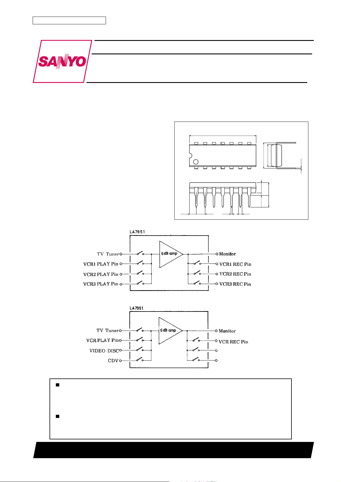
The LA7951 Video Switch is a solid-state 4-input 4-output
video switch ideally suited for use as a video selector switch
in multiple-source video systems and multiple VCR video
editing systems.
The Switching logic, coupled with built-in video amplifier, ripple filter and 75Ω output driver facilitate a minimum parts count video switching subsystem. The solidstate switches feature low crosstalk and wide bandwidth.
The LA7951 operates from a single 12V power supply , and
is available in 14-pin plastic DIPs.
Features
• 4-input 4-output multi-functional video switch.
• Low crosstalk, wide bandwidth.
• Internal 6 dB video amplifier.
• Ripple filter.
• 75Ω output driver for video monitor (COMMON OUT).
Package Dimensions
unit:mm
3003B-DIP14
[LA7951]
19.0
14
1
(1.88)
2.54
0.48
8
6.4
7.62
0.25
7
(3.0)
3.65max
3.4
0.51min
1.2
SANYO : DIP14
Figure 1. Editing System Switch Connections
Figure 2. Video Selector Switch Connections
12501TN (KT)/N050JK/8258YT, TS No.2868–1/4
Page 2
LA7951
Specifications
Maximum Ratings at Ta = 25˚C
retemaraPlobmySsnoitidnoCsgnitaRtinU
egatlovylppusmumixaMV
egatlovtupnilortnocmumixaM
1tnerructuptuolangismumixaMI
2tnerructuptuolangismumixaM
noitapissidrewopelbawollAxamdP 52.1Wm
erutarepmetgnitarepOrpoT 57+ot02–
erutarepmetegarotSgtsT 521+ot55–
Operating Conditions at Ta = 25˚C
retemaraPlobmySsnoitidnoCsgnitaRtinU
egatlovylppusdednemmoceRV
egnaregatlovgnitarepOV
Operating Characteristics at Ta = 25˚C, VCC=12V
retemaraPlobmySsnoitidnoC
niardtnerructnecseiuQICCDNGot31,9,6snip,nepo41,8,7sniP025.7273Am
egatlovsaibniptupnIV
1egatlovsaibniptuptuOV
2egatlovsaibniptuptuOV
1HegatlovdlohserhtlortnoCV
2HegatlovdlohserhtlortnoCV
1LegatlovdlohserhtlortnoCV
2LegatlovdlohserhtlortnoCV
1tnerructupnilortnoCI
2tnerructupnilortnoCI
1niagegatloV1VGV,zHM1=f
2niagegatloV2VGV,zHM1=f
scitsiretcarahcycneuqerFfVG
egatlovesiontuptuOV
1egnarcimanydtuptuO1RDV,zHk01=f
2egnarcimanydtuptuO2RDV,zHk01=f
1klatssorC1TCV,zHM4=f
2klatssorC2TCV,zHM4=f
Note ) Measured output terminated with 75Ω. Current flowing into IC is taken as plus (+). Parameter 1 refers to the COMMON OUT signal output
and parameter 2 to the OUT1 to OUT3 signal outputs.
xam 41V
4
V6,xam
V9,xam
V31xam
xam 5–Am
1
I7,xam
I8,xam
I41xam
Ta≤50˚C
CC
po 2.31ot9V
CC
nimpytxam
3V,5V,01V,21
1
7V,8V,41
H6
V,
H9
H31
L6
V,
L9
L31
6
9I,31
N
V6V5=23.05.0Am
V9V=
V5=005–Aµ
31
O
O
V,zHk001=f
O
.etoN
O
O
O
O
.etoNeeS,p-pV1=5.0–5.0+5.1+Bd
.etoNeeS,p-pV1=7.0–3.0+3.1+Bd
eeS,zHM01=f,Bd0=p-pV1=
.etoNeeS,zHM2.4otzHk01=FPB5.00.1smrVm
.etoNeeS,p-pV5.1=5.02.1%
.etoNeeS,p-pV5.1=0.10.2%
.etoNeeS,p-pV1=05–55–Bd
.etoNeeS,p-pV1=02–04–Bd
6.21.36.3V
6.43.50.6V
3.30.47.4V
3.2V
0.3V
08.0V
05.1V
3–1–Bd
sgnitaR
V
CC
02–Am
21V
CC
CC
V
˚C
˚C
tinU
V
V
No.2868–2/4
Page 3
LA7951
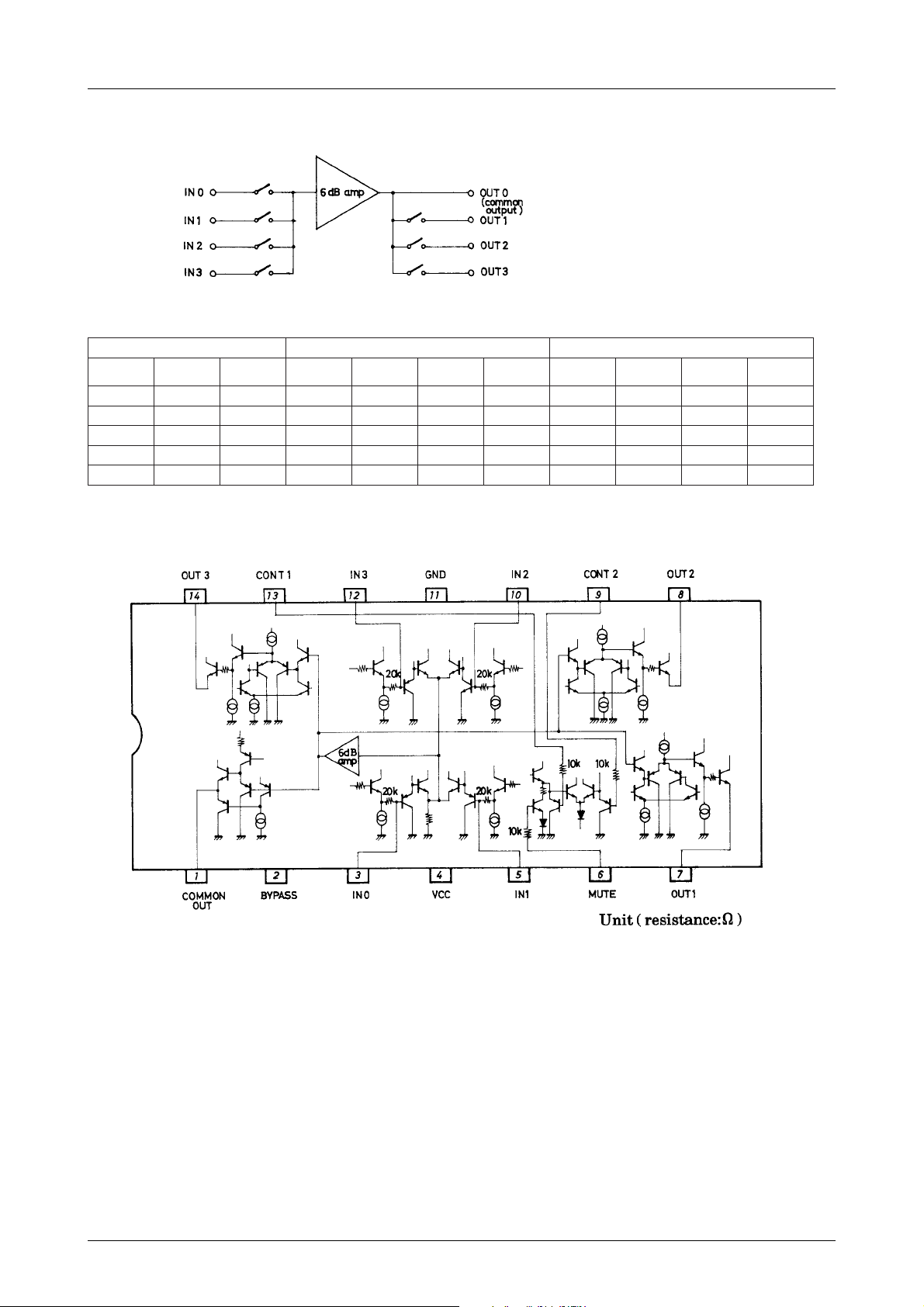
Video Switch Block Diagram
Switching Functions
lortnoCtupnItuptuO
ETUM
)6niP(
L–– FFOFFOFFOFFONOFFOFFOFFO
HLL NOFFOFFOFFONONONONO
HLH FFONOFFOFFONOFFONONO
HHL FFOFFONOFFONONOFFONO
HHH FFOFFOFFONONONONOFFO
1
)31niP(
2
)9niP(
0
)3niP(
1
)5niP(
2
)01niP(
3
)21niP(
NOMMOC
)1niP(
1
)7niP(
2
)8niP(
3
)41niP(
Equivalent Circuit Block Diagram
No.2868–3/4
Page 4
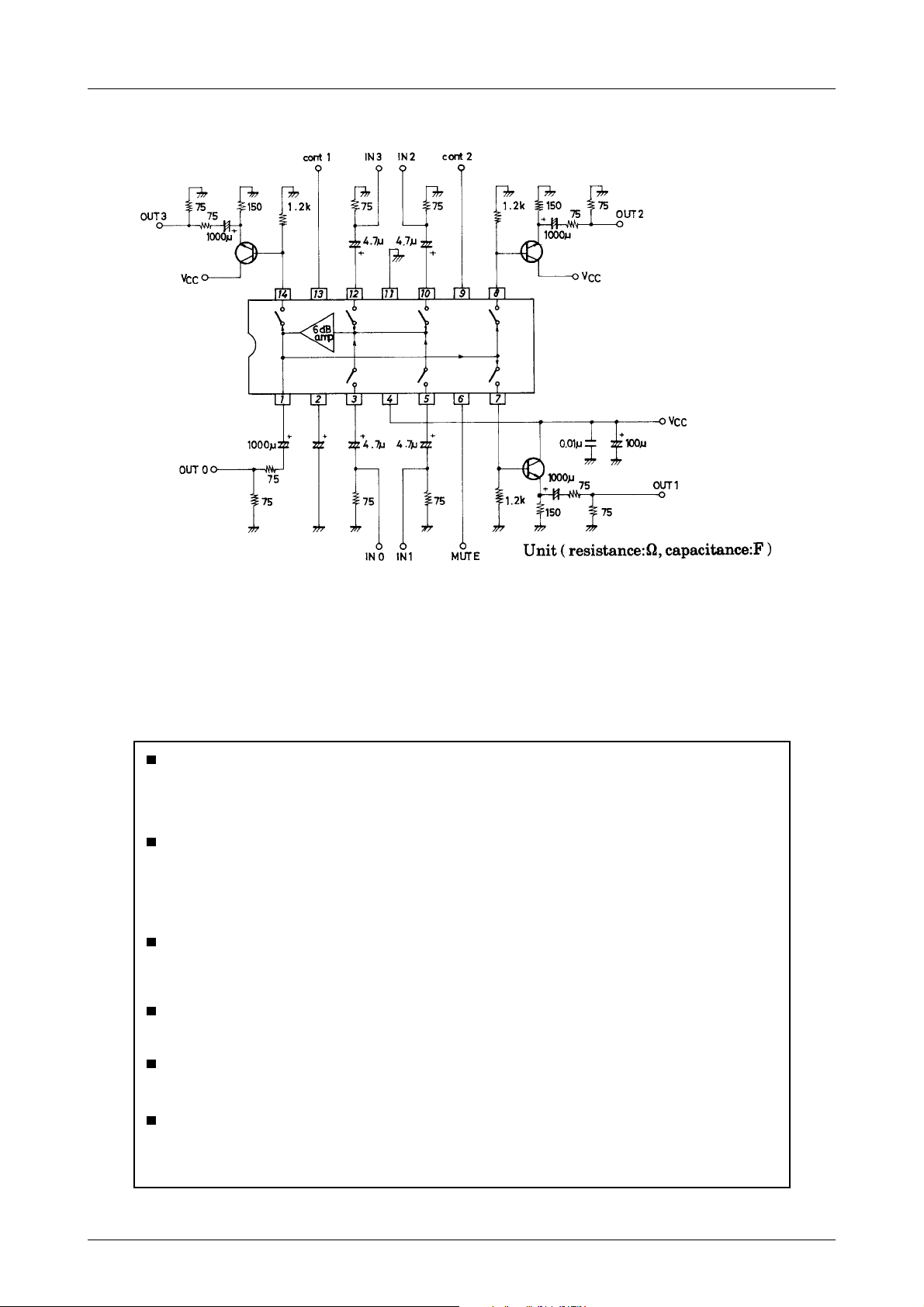
Sample Applicationn Circuit
LA7951
The power supply decoupling capacitor should be mounted as close to the LA7951 as physically possible.
Specifications of any and all SANYO products described or contained herein stipulate the performance,
characteristics, and functions of the described products in the independent state, and are not guarantees
of the performance, characteristics, and functions of the described products as mounted in the customer's
products or equipment. To verify symptoms and states that cannot be evaluated in an independent device,
the customer should always evaluate and test devices mounted in the customer's products or equipment.
SANYO Electric Co., Ltd. strives to supply high-quality high-reliability products. However, any and all
semiconductor products fail with some probability. It is possible that these probabilistic failures could
give rise to accidents or events that could endanger human lives, that could give rise to smoke or fire,
or that could cause damage to other property. When designing equipment, adopt safety measures so
that these kinds of accidents or events cannot occur. Such measures include but are not limited to protective
circuits and error prevention circuits for safe design, redundant design, and structural design.
In the event that any or all SANYO products(including technical data,services) described or
contained herein are controlled under any of applicable local export control laws and regulations,
such products must not be exported without obtaining the export license from the authorities
concerned in accordance with the above law.
No part of this publication may be reproduced or transmitted in any form or by any means, electronic or
mechanical, including photocopying and recording, or any information storage or retrieval system,
or otherwise, without the prior written permission of SANYO Electric Co. , Ltd.
Any and all information described or contained herein are subject to change without notice due to
product/technology improvement, etc. When designing equipment, refer to the "Delivery Specification"
for the SANYO product that you intend to use.
Information (including circuit diagrams and circuit parameters) herein is for example only ; it is not
guaranteed for volume production. SANYO believes information herein is accurate and reliable, but
no guarantees are made or implied regarding its use or any infringements of intellectual property rights
or other rights of third parties.
This catalog provides information as of January, 2001. Specifications and information herein are subject
to change without notice.
PS No.2868–4/4
 Loading...