

Page 1
Any and all SANYO products described or contained herein do not have specifications that can handle
applications that require extremely high levels of reliability, such as life-support systems, aircraft’s
control systems, or other applications whose failure can be reasonably expected to result in serious
physical and/or material damage. Consult with your SANYO representative nearest you before using
any SANYO products described or contained herein in such applications.
SANYO assumes no responsibility for equipment failures that result from using products at values that
exceed, even momentarily, rated values (such as maximum ratings, operating condition ranges,or other
parameters) listed in products specifications of any and all SANYO products described or contained
herein.
Monolithic Linear IC
Closed Caption Signal (US specifications)
Extraction IC
Ordering number:ENN4616
LA7945N
SANYO Electric Co.,Ltd. Semiconductor Company
TOKYO OFFICE Tokyo Bldg., 1-10, 1 Chome, Ueno, Taito-ku, TOKYO, 110-8534 JAPAN
Overview
The LA7945N extracts the closed caption signal overlapped
in the video signal vertical retrace period and transfers the
data and clock signal to a decoder IC. This IC requires the
use of either an add-on type decoder, such as the LC7458B
or 7457A (for I2C), or a microcontroller type decoder, such
as the LC8640XX.
Functions
• Synchronization separation.
• VCO
• Vertical countdown.
• Horizontal countdown.
• Data slicing.
• Dual loop AFC.
• Field discrimination.
• Lock detection
• Vertical/horizontal pulse output.
Features
• Adoption of a dual loop AFC allows the LA7945N to stably extract the caption signal.
• Provides the pulse outputs required by caption decoder
ICs.
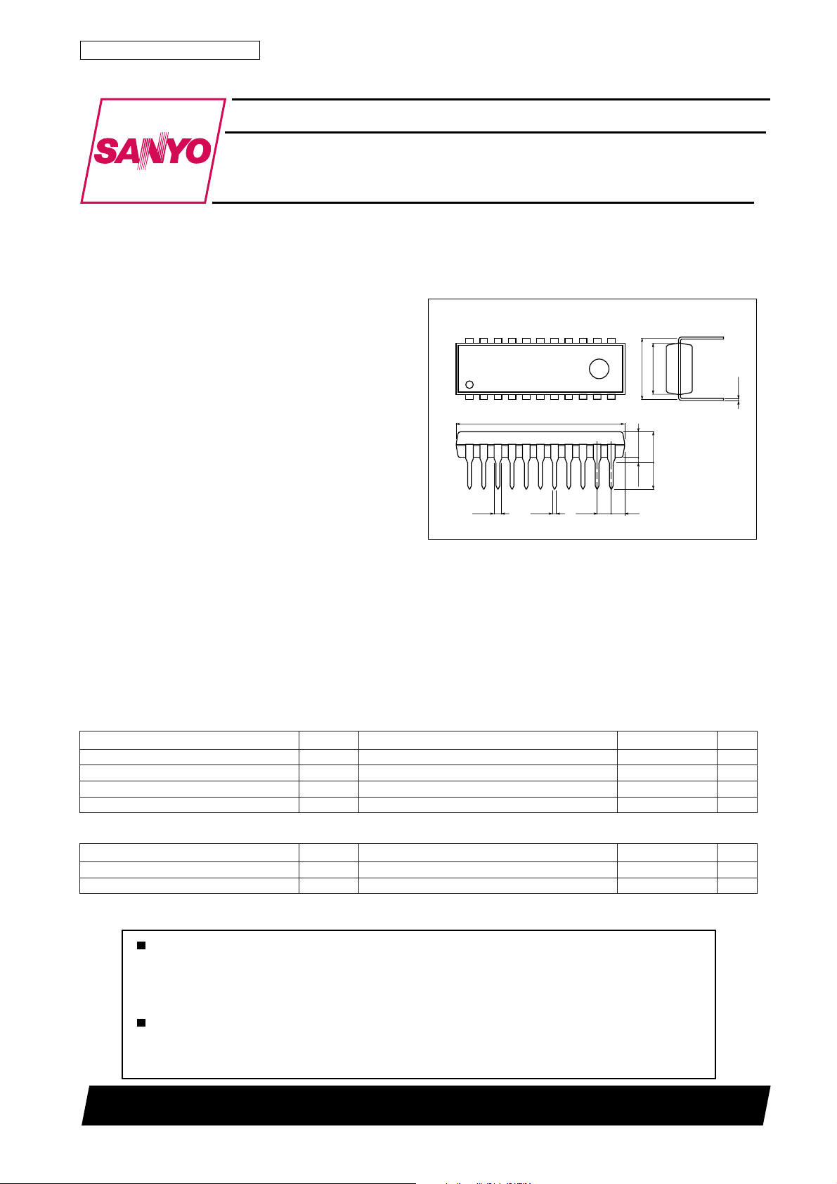
Package Dimensions
unit:mm
3059-DIP22S
[LA7945N]
22 12
6.4
7.62
111
0.95 0.48
21.2
1.78
3.25
3.9max
3.3
0.51min
1.7
SANYO : DIP22S
0.25
Specifications
Maximum Ratings at Ta = 25˚C
retemaraPlobmySsnoitidnoCsgnitaRtinU
egatlovylppusrewopmumixaMV
noitapissidrewopelbawollAxamdP 052Wm
erutarepmetgnitarepOrpoT 07+ot01–
erutarepmetegarotSgtsT 051+ot55–
Operating Conditions at Ta = 25˚C
retemaraPlobmySsnoitidnoCsgnitaRtinU
egatlovylppusrewopdednemmoceRV
egnaregatlovylppusrewopgnitarepOV
xam 7V
CC
Ta≤70˚C
CC
po 5.5ot5.4V
CC
12501TN (KT)/D2593TS B8-0107 No.4616–1/9
˚C
˚C
5V
Page 2
LA7945N
Electrical and Operating Characteristics at Ta = 25˚C, VCC=5.0V, Input signal : sync-white 1.0V
retemaraPlobmySsnoitidnoC
egnarni-lluplatnoziroHf
ycneuqerfgninnur-eerflatnoziroHf
egatlovgnipmalctupnIV
leveldlohserhtretlifKCOLHV
tuptuonoitarapesnoitazinorhcnyS
retlifKCOLH
tuptuoataD
tuptuokcolC
tuptuoH12
tuptuoE/O
tuptuoesluplatnoziroH
tuptuoesluplacitreV
levellangistupnIV
emittratsNI-NUR-KLCT
niardtnerruCI
levelhgiHV
levelwoLV
levelhgiHV
levelwoLV
levelhgiHV
levelwoLV
levelhgiHV
levelwoLV
levelhgiHV
levelwoLV
htdiwesluPV
levelhgiHV
levelwoLV
htdiwesluPV
levelhgiHV
levelwoLV
htdiwesluPV
levelhgiHV
levelwoLV
htdiwesluPV
PMLC
HKLC
LKLC
HH12
LH12
WH12
HEO
LEO
WEO
HSH
LSH
WSH
HTSR
LTSR
WTSR
NI
TS
CC
Note : Must not be pulled in to any frequency other than fH.
The pin 11 capacitor should be 100pF ±5%.
The pin 12 resistor should be 15kΩ ±1%.
nimpytxam
LLUPH
EERFH
HTKCOL
HCNYS
LCNYS
HKCOL
LKCOL
HATAD
LATAD
sgnitaR
5.1±zHk
3.517.513.61zHk
3.25.27.2V
3.25.27.2V
0.42.40.5V
08.00.1V
0.42.40.5V
08.00.1V
0.42.40.5V
08.00.1V
0.42.40.5V
08.00.1V
0.42.40.5V
08.00.1V
065607sµ
0.42.40.5V
08.00.1V
4.617.610.71sm
0.42.40.5V
08.00.1V
4.77.70.8sµ
0.42.40.5V
08.00.1V
8.038.138.23sµ
6–03+Bd
6.66.76.8sµ
0.410.810.22Am
tinU
No.4616–2/9
Page 3
LA7945N
Test Conditions
retemaraPlobmyStnioptseTdohtemtseT
fycneuqerfehtyraV
egnarni-lluplatnoziroHf
ycneuqerfgninnur-eerflatnoziroHf
egatlovgnipmalctupnIV
leveldlohserhtretlifKCOLHV
tuptuonoitarapesnoitazinorhcnyS
retlifKCOLH
tuptuoataD
tuptuokcolC
levelhgiHV
levelwoLV
levelhgiHV
levelwoLV
levelhgiHV
levelwoLV
levelhgiHV
levelwoLV
levelhgiHV
tuptuoH12
levelwoLV
htdiwesluPV
levelhgiHV
tuptuoE/O
levelwoLV
htdiwesluPV
levelhgiHV
tuptuoesluplatnoziroH
levelwoLV
htdiwesluPV
levelhgiHV
tuptuoesluplacitreV
levelwoLV
htdiwesluPV
levellangistupnIV
emittratsNI-NUR-KLCT
niardtnerruCI
LLUPH
EERFH
PMLC
HTKCOL
HCNYS
LCNYS
HKCOL
LKCOL
HATAD
LATAD
HKLC
LKLC
HH12
LH12
WH12
HEO
LEO
WEO
HSH
LSH
WSH
HTSR
LTSR
WTSR
NI
TS
CC
01dna2sniP
01niP
71niP.epocsollicsonahtiwlevellatsedepehterusaeM
7niP
1
*2niP
1
*7niP
2,1
*3niP
2,1
*5niP
1
*1niP
1
*6niP
1
*01niP
1
*9niP
,1snipfohcaE
2
*6dna,5,3
,1snipfohcaE
3,2
*6dna,5,3
2
*61niP
.langis
.gnidoced
Note : 1. Connect a 20kΩ resistor between the pin being measured and VCC, and also connect a 20kΩ from that measurement pin to GND.
2. During measurement, this pin carries the closed caption encoded signal.
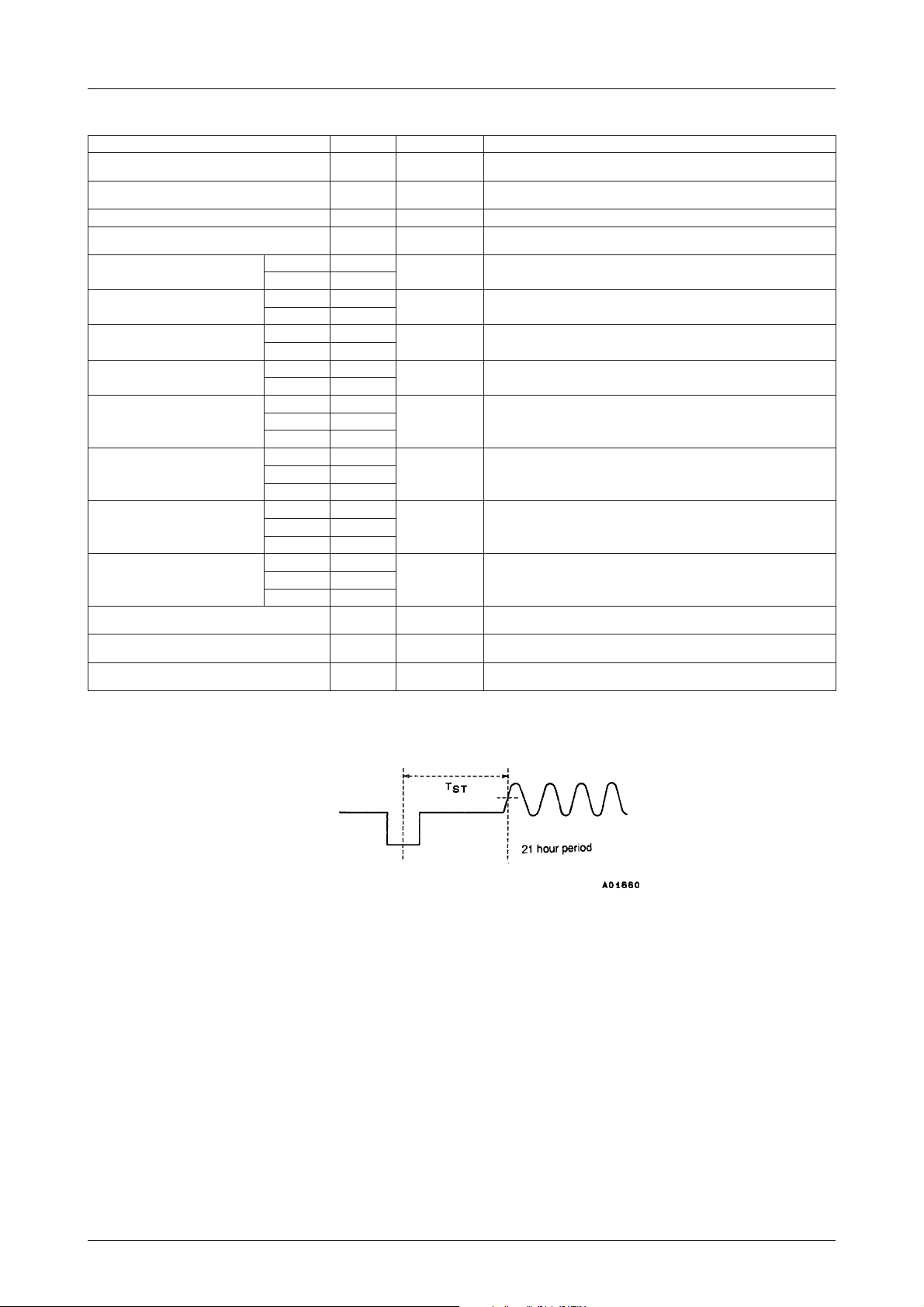
3. Time TST is shown in the figure below.
H
.epocsollicsonagnisuskcol01dna2snipfoesahpeht
.egatlovtahtgniyravdna8nipotegatlov
.epocsollicsonahtiwdoirep
.epocsollicsonahtiwdoirep
.epocsollicsonahtiwdoirep
.epocsollicsonahtiwdoirep
.yltcerrocgnitarepoerastuptuo6dna
.yltcerrocgnitarepoerastuptuo6dna,5,3,1nip
erehwtniopehterusaemdnalangistupniehtfo
onsierehtnehwycneuqerfehterusaemotretnuocycneuqerfaesU
CDagniylppaybhgihseog7niphcihwtaegatlovehterusaeM
.epocsollicsonahtiwslevelwoldnahgih2nipehterusaeM
.epocsollicsonahtiwslevelwoldnahgih7nipehterusaeM
.epocsollicsonahtiwslevelwoldnahgih3nipehterusaeM
.epocsollicsonahtiwslevelwoldnahgih5nipehterusaeM
levelhgihehtfohtgnelehtdnaslevelwoldnahgih1nipehterusaeM
levelhgihehtfohtgnelehtdnaslevelwoldnahgih6nipehterusaeM
levelhgihehtfohtgnelehtdnaslevelwoldnahgih01nipehterusaeM
levelhgihehtfohtgnelehtdnaslevelwoldnahgih9nipehterusaeM
,5,3,1nipehttahtmrifnocdna,71nipottupnilevellangisehtyraV
ehttahtmrifnocdna,NI-NUR-KLCdnaCNYSneewtebemitehtyraV
gnirudtnerrucehterusaemdna,61nipotretemtnerrucatcennoC
No.4616–3/9
Page 4

Test Circuit Diagram
LA7945N
Application Circuit Diagram
No.4616–4/9
Page 5

LA7945N
Pin Descriptions
* The peripheral circuit for the pins described below is shown in figure 1.
Either a resistor or a fixed current supply is connected to the lower side
(the side away from the pin) of the differential amplifier.
Pin 1 (21H OUT) : R=18kΩ. This signal goes high during the 21H and
Pin 2 (sync SEP) : R=9kΩ. Synchronization separation output, see pin
Pin 3 (DATA OUT) : I≈280µA.
Pin 5 (CLOCK OUT) : R=9kΩ. A clock output whose phase matches that
Pin 6 (O/E OUT) : R=18kΩ. Field discrimination signal. High on odd
Pin 7 (H LOCK OUT) : I≈50µA.
Pin 9 (V PULSE OUT) : R=18kΩ. Set low during the 0.5H period
Pin 10 (H PULSE OUT) : R=18kΩ. Outputs a low signal synchronized
Figure 1
• Pin 8 (H LOCK FILTER) : The H LOCK detection filter is connected to this pin.
Pin 8 is charged when the H gate and Sync phases match, and this voltage
is compared and output to pin 7. The resistor R1 is used for discharge. The
time from internal VCO locking until pin 7 goes high, and the time from
lock release to the pin going low can be adjusted by changing the values of
C1 and R1. If the pin 7 H LOCK OUT output is not used, C1 and R1 will
be unnecessary.
284H periodes. The fall of this signal is taken as the completion of
data transfer.
19.
Outputs the data overlapped with the vertical retrace period.
of DATA OUT.
fields.
A resistor and capacitor are connected to pin 8, and this pin goes
high when the internal VCO and the input signal are synchronized.
synchronized with the vertical synchronization signal.
with the horizontal synchronization signal.
Figure 2 : Pin 8 (H LOCK FILTER) Peripheral Circuit
• Pin 11 (VCO C) : The capacitor for the 32fH VCO is connected to this pin. (Error : 5%)
The LA7945N generates the 32fH oscillation not by using a ceramic resonator, but by char ging this capacitor with the f ixed cur rent def ined by the resistance connected at pin 12. The horizontal pulses and the clock output from
pin 5 are generated using this oscillator as a reference.
Figure 3 : Pin 11 (VCO C) Peripheral Circuit
No.4616–5/9
Page 6

LA7945N
• Pin 12 (VCO R) : The capacitor for the 32fH VCO is connected to this pin. (Error : 1%)
The resistor defines the current that charges the pin 11 capacitor . A DC voltage of 2/3 that of VCC is output from pin 12.
Figure 4 : Pin 12 (VCO R) Peripheral Circuit
• Pin 13 (AFC1) : The horizontal AFC filter is connected to this pin.
Figure 5 : Pin 13 (AFC1) Peripheral Circuit
Although the ability to follow horizontal fluctuarions improves as R1 increases, the holding power is reduced. Select this value according to the application circuit. Since the closed caption signal is overlapped with 21H, the
VCO in this IC is influenced by signals such as the vertical synchronization
signal and the copy guard signal. The values of C2 and C3 should be determined so that the VCO is stable with respect to these signals. To stabilize pin
13 at a voltage of about 2.7V (when VCC=5V) with no input, the ratio of C2
and C3 should be set so that this voltage takes on a value close to the of pin
13 when power is first applied.
No.4616–6/9
Page 7

LA7945N
• Pin 14 (AFC2) : Used for phase adjustment of the internal VCO CLOCK and CLK-RUN-IN
A signal is output from pin 14 only during the 21H CLK-RUN-IN period,
and the phase is adjusted by controlling the fixed current determined by the
15kΩ resistor on pin 12 only during that period.
• Pin 15 (CLOCK PHASE) : CLOCK-RUN-IN phase compensation pin.
Only the CLK-RUN-IN signal during the vertical retrace period is extracted
and passed to the multiplier described above. The phase of the clock output
from pin 5 can be adjusted by the value of the capacitor (C1) connected to
this pin.
Figure 6 : Pin 14 (AFC2) and Pin 15 (CLOCK PHASE) Peripheral Circuit
• Pin 17 (VIDEO IN) : The video input pin. (sync-white 1 Vp-p)
Pin 17 is designed to clamp the pedestal level at 1/2 VCC. Since C1 also
functions as the clamping capacitor, it should be driven with a low impedance (less than 500Ω). The low field performance can be improved by adding an LPF such as R1 and C2. If this LPF is used, R1 must be a low resistance that can meet the conditions described above.
Figure 7 : Pin 17 (VIDEO IN) Peripheral Circuit
No.4616–7/9
Page 8

LA7945N
• Pin 18 (DATA LPF) : The data slice LPF is connected to this pin.
A signal is output from pin 18 during the vertical retrace period CLK-RUNIN period, and an LPF, which is used to detect the average value of CLKRUN-IN (to be used as the slice level), is connected to this pin.
Figure 8 : Pin 18 (DATA LPF) Peripheral Circuit
• Pin 19 (PEAK HOLD) : The synchronization separator peak hold capacitor is connected to this pin.
The IC holds the peak value of sync on pin 19, and performs synchronization
separation using 1/2 this level as the reference. This output is output from
pin 2.
Figure 9 : Pin 19 (PEAK HOLD) Peripheral Circuit
• Pin 20 (V SEP R) : The resistor that determines the vertical synchronization separation is connected to this pin.
The LA7945N performs vertical synchronization separation by charging an
internal capacitor using the fixed current determined by the resistor connected to this pin as the reference. The pin 20 DC voltage is 1/4 V
CC.
Figure 10 : Pin 20 (V SEP R) Peripheral Circuit
No.4616–8/9
Page 9

LA7945N
• Pin 21 : The vertical synchronization separation output pin.
The signal passed to the vertical C/D from vertical synchronization separation is output from pin 21. Since vertical C/D is I2L, a signal of between 0
and 0.7V is output. This pin is normally left open. The vertical C/D start
position can be changed by an external override input.
Figure 11 : Pin 21 Peripheral Circuit
• Pin 22 : This pin determines whether or not the horizontal count for vertical C/D is changed every frame when the start bit is not detected.
When this pin is grounded, 21H is fixed, and it functions when open.
Ground this pin when captions are used.
Figure 12 : Pin 22 Peripheral Circuit
Specifications of any and all SANYO products described or contained herein stipulate the performance,
characteristics, and functions of the described products in the independent state, and are not guarantees
of the performance, characteristics, and functions of the described products as mounted in the customer's
products or equipment. To verify symptoms and states that cannot be evaluated in an independent device,
the customer should always evaluate and test devices mounted in the customer's products or equipment.
SANYO Electric Co., Ltd. strives to supply high-quality high-reliability products. However, any and all
semiconductor products fail with some probability. It is possible that these probabilistic failures could
give rise to accidents or events that could endanger human lives, that could give rise to smoke or fire,
or that could cause damage to other property. When designing equipment, adopt safety measures so
that these kinds of accidents or events cannot occur. Such measures include but are not limited to protective
circuits and error prevention circuits for safe design, redundant design, and structural design.
In the event that any or all SANYO products(including technical data,services) described or
contained herein are controlled under any of applicable local export control laws and regulations,
such products must not be exported without obtaining the export license from the authorities
concerned in accordance with the above law.
No part of this publication may be reproduced or transmitted in any form or by any means, electronic or
mechanical, including photocopying and recording, or any information storage or retrieval system,
or otherwise, without the prior written permission of SANYO Electric Co. , Ltd.
Any and all information described or contained herein are subject to change without notice due to
product/technology improvement, etc. When designing equipment, refer to the "Delivery Specification"
for the SANYO product that you intend to use.
Information (including circuit diagrams and circuit parameters) herein is for example only ; it is not
guaranteed for volume production. SANYO believes information herein is accurate and reliable, but
no guarantees are made or implied regarding its use or any infringements of intellectual property rights
or other rights of third parties.
This catalog provides information as of January, 2001. Specifications and information herein are subject
to change without notice.
PS No.4616–9/9
 Loading...