

Page 1
Any and all SANYO products described or contained herein do not have specifications that can handle
applications that require extremely high levels of reliability, such as life-support systems, aircraft’s
control systems, or other applications whose failure can be reasonably expected to result in serious
physical and/or material damage. Consult with your SANYO representative nearest you before using
any SANYO products described or contained herein in such applications.
SANYO assumes no responsibility for equipment failures that result from using products at values that
exceed, even momentarily, rated values (such as maximum ratings, operating condition ranges,or other
parameters) listed in products specifications of any and all SANYO products described or contained
herein.
Monolithic Linear IC
Peripheral Circuit for TV/VCR Frequency
Synthesizer Channel Select System
Ordering number:ENN4038
LA7916
SANYO Electric Co.,Ltd. Semiconductor Company
TOKYO OFFICE Tokyo Bldg., 1-10, 1 Chome, Ueno, Taito-ku, TOKYO, 110-8534 JAPAN
Overview
The LA7916 contains CPU/PLL-excluded peripheral circuits such as switch, +5V power supply (with RST), sync
detector, low-pass filter for color TV/VCR frequency synthesizer channel select system use.
Functions
• Band switch (2-input 4-output).
• Video signal, flyback pulse, AFT output-used detection
of tuning mode and horizontal sync mode.
• +5V power supply, with RST ouput (for CPU).
• Operational amplifier for low-pass filter (for frequency
synthesizer).
Features
• The band switch truth table can be changed in a short
period of time at the user’s option.
• The band switch is of pnp output type which need not be
driven externally.
• The operational amplifier for low-pass filter is excellent
in pulse response because of its high-impedance input
pin.
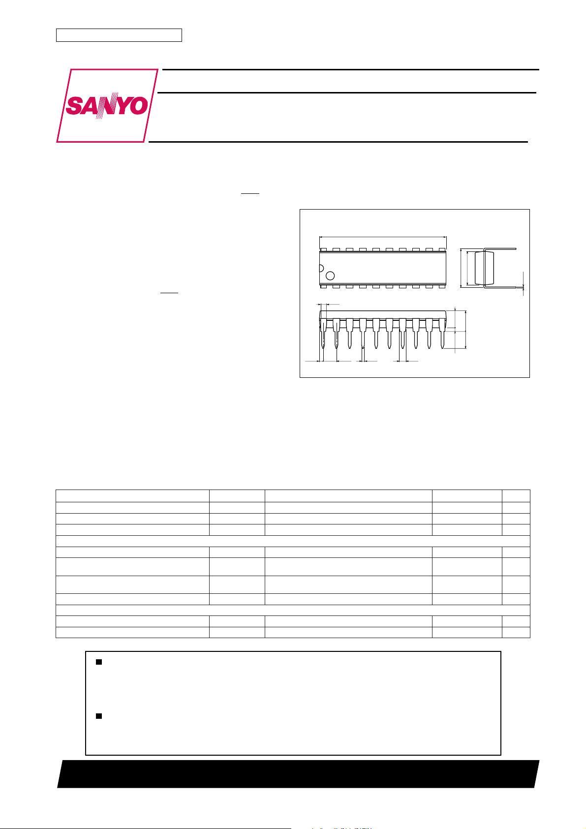
Package Dimensions
unit:mm
3021C-DIP20
[LA7916]
24.0
20
1
1.0
(0.57)
2.54
0.5
1.2
11
7.62
10
(3.25)
0.51min
SANYO : DIP20
6.4
0.25
3.9max
3.3
Specifications
Maximum Ratings at Ta = 25˚C
retemaraPlobmySsnoitidnoCsgnitaRtinU
noitapissidrewopelbawollAxamdP 077Wm
erutarepmetgnitarepOrpoT 56+ot02–
erutarepmetegarotSgtsT 521+ot55–
]noitceshctiwsdnaB[
V
1CC
V
2CC
tnerructuptuoV5+I
egatlovylppusmumixamV
tnerrucdaolmumixaM
egatlovdeilppamumixaM
)tupni(egatlovdeilppamumixaM
]noitcesylppusrewopV5+[
egatlovylppusmumixamV
I41I,
I61I,
V41V,
V61V,
V
6
31
51
71
01
8
Ta≤65˚C
xam 51V
,xam
xam
,xam
51
xam
71
V,xam
xam
7
xam 51V
xam 83–Am
ffotuptuO 51–V
V
V41=21V
1CC
12501TN (KT)/N261TH No.4038–1/4
˚C
˚C
05–Am
Continued on next page.
Page 2
Continued from preceding page.
retemaraPlobmySsnoitidnoCsgnitaRtinU
]noitcesnoitcetedgninuT[
egatlovtupnimumixaMV
egatlovtupnimumixaMV
)ytiralopevitagen(egatlovtupnimumixaMV–
egatlovecnereffidrotarapmocmumixaMV
tnerructuptuomumixaMI
]noitcesreifilpmalanoitarepO[
egatlovdeilppamumixaMV
egatlovtupnimumixaMV
Operating Conditions at Ta = 25˚C
retemaraPlobmySsnoitidnoC
egnaregatlovylppuS
gninutnitnerructuptuodednemmoceR
noitcesnoitceted
lanoitareponitnerrucdaoldednemmoceR
noitcesreifilpma
rotarapmocfoegnargnittesdednemmoceR
noitcesnoitcetedgninutniegatlov
LA7916
xam 5.3V
2
xam V
3
xam 4.1–V
2
91V-02
xam 3–Am
1
xam 53V
21
xam 9.5V
11
sgnitaR
nimpytxam
V
01
V
31
I4I,
5
I
21
V
91
0.9210.41V
0.9210.41V
35Am
7.20.7V
V
1CC
6V
tinU
3Am
Operating Characteristics at Ta = 25˚C
retemaraPlobmySsnoitidnoC
]noitceshctiwsdnaB[
niardtnerructnecseiuQI
egatlovnoitarutastuptuOtas4ot1FAm04–=oI07.0V
egatlovlevel-hgihtupnI
egatlovlevel-woltupnI
tnerrucegakaeltuptuOI
]noitcesylppusrewopV5+[
niardtnerructnecseiuQI
egatlovtuptuoV5+V
egatlovtuptuoTSRV
]noitcesnoitcetedginuT[
egatlovdlohserhttupnIV
egatlovrotarapmoCV
egatlovhgihrotarapmocwodniWV
egatlovwolrotarapmocwodniWV
egatlovnoitarutastuptuO
tnerructuptuoretlifssap-woLI
tnerructratsnoitarapescnySI
]noitcesreifilpmalanoitarepO[
egatlovnoitarutastuptuOV
egatlovdlohserhttupnIV
tnerructupnII
V
V
V4tasAm2=knisI033.07.0V
V5tasAm2=knisI033.07.0V
sgnitaR
nimpytxam
1CC
V,
HT6
HT7
V,
LT6
LT7
LF
2CC
8
9
HT2
91C
HC
LC
LO
HT1
21
11
V51– 05–Aµ
I
Am03–=5.45.5V
8
tasI9Aµ001–=5.45.5V
tas03.0V
HT11
0.61Am
2.2V
08.0V
6.3Am
4.027.05.1V
7.30.43.4V
7.50.63.6V
7.20.33.3V
08.1–09.0–Am
051–Aµ
0.24.2V
02An
tinU
Band Switch Truth Table
tupnItuptuO
A
)7niP(
L
H
L
H
B
)6niP(
L
L
H
H
1F
)41niP(
H
Z
Z
Z
2F
)51niP(
Z
H
Z
Z
3F
)61niP(
Z
Z
H
Z
4F
)71niP(
Z
Z
Z
H
No.4038–2/4
Page 3

Operation of Tuning Detection Section
edoMgninuTtuptuOFPLTFA1TUO2TUO
dezinorhcnysnUL
dezinorhcnySH
L-TFA
C-TFA
H-TFA
L-TFA
C-TFA
H-TFA
AFT -L : V
AFT -C : VCL<V
AFT -H : V
L
L
L
H
H
L
LA7916
L
L
L
L
H
H
AFT<VCL
AFT<VCH
AFT>VCH
+5V Power Supply, RST Output
When +5V output V8 becomes approximately 4V at the time of application of power , the reset signal is
delivered at pin 9. The r eset signal can be delayed by a capacitor (recommended v alue : 1µF) externally
connected to RST output V9.
No.4038–3/4
Page 4

Sample Application Circuit
LA7916
VCR application : In VCR applications without flyback pulse, connected pin 2 to VCC through a resistor.
Specifications of any and all SANYO products described or contained herein stipulate the performance,
characteristics, and functions of the described products in the independent state, and are not guarantees
of the performance, characteristics, and functions of the described products as mounted in the customer's
products or equipment. To verify symptoms and states that cannot be evaluated in an independent device,
the customer should always evaluate and test devices mounted in the customer's products or equipment.
SANYO Electric Co., Ltd. strives to supply high-quality high-reliability products. However, any and all
semiconductor products fail with some probability. It is possible that these probabilistic failures could
give rise to accidents or events that could endanger human lives, that could give rise to smoke or fire,
or that could cause damage to other property. When designing equipment, adopt safety measures so
that these kinds of accidents or events cannot occur. Such measures include but are not limited to protective
circuits and error prevention circuits for safe design, redundant design, and structural design.
In the event that any or all SANYO products(including technical data,services) described or
contained herein are controlled under any of applicable local export control laws and regulations,
such products must not be exported without obtaining the export license from the authorities
concerned in accordance with the above law.
No part of this publication may be reproduced or transmitted in any form or by any means, electronic or
mechanical, including photocopying and recording, or any information storage or retrieval system,
or otherwise, without the prior written permission of SANYO Electric Co. , Ltd.
Any and all information described or contained herein are subject to change without notice due to
product/technology improvement, etc. When designing equipment, refer to the "Delivery Specification"
for the SANYO product that you intend to use.
Information (including circuit diagrams and circuit parameters) herein is for example only ; it is not
guaranteed for volume production. SANYO believes information herein is accurate and reliable, but
no guarantees are made or implied regarding its use or any infringements of intellectual property rights
or other rights of third parties.
This catalog provides information as of January, 2001. Specifications and information herein are subject
to change without notice.
PS No.4038–4/4
 Loading...