Ordering number: EN 4957A
Monolithic Linear IC
LA7890
RGB Cutoff Adjustment IC
Overview
The LA7890 is a DC-controlled, CRT display RGB cutoff
adjustment IC. It can be used for a wide range of applications,
regardless of whether they employ a Trinitron tube or a
dot-matrix tube display.
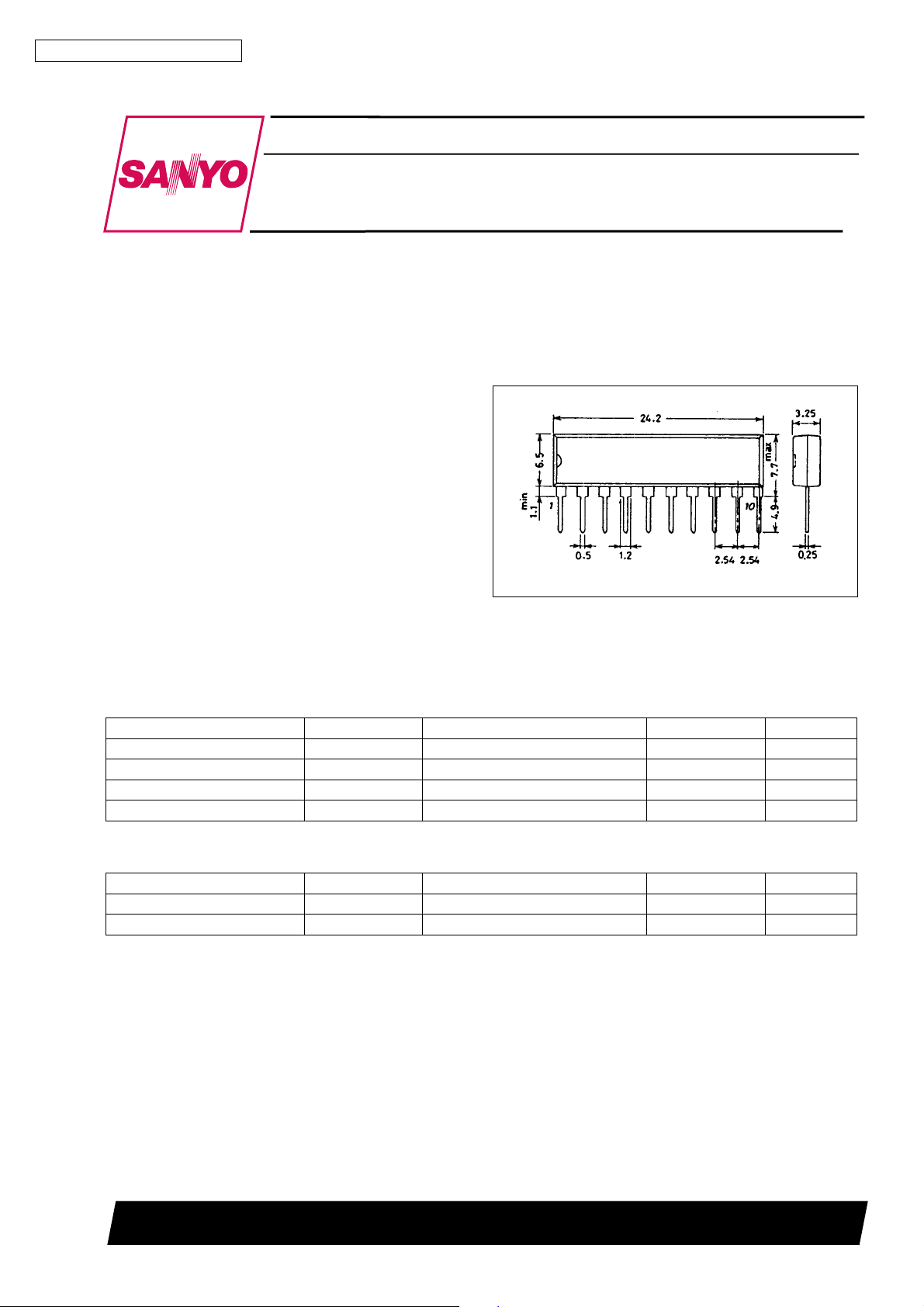
Package Dimensions
unit : mm
3043A-SIP10
[LA7890]
Function
.
Operational amplifier
Features
.
DC control
.
Temperature drift stability
.
100 V maximum supply voltage
SANYO : SIP10
Specifications
Maximum Ratings at Ta = 25°C
Parameter Symbol Conditions Ratings Unit
Maximum supply voltage V
Allowable power dissipation Pd max Ta % 75°C 400 mW
Operating temperature Topr –10 to +75 °C
Storage temperature Tstg –55 to +150 °C
max 100 V
CC
Recommended Operating Conditions at Ta = 25°C
Parameter Symbol Conditions Ratings Unit
Recommended supply voltage V
Operating supply voltage V
CC
op 60 to 90 V
CC
80 V
SANYO Electric Co.,Ltd. Semiconductor Bussiness Headquarters
TOKYO OFFICE Tokyo Bldg., 1-10, 1 Chome, Ueno, Taito-ku, TOKYO, 110 JAPAN
O3096HA(II)/41495TH(ID) No.4957-1/3

LA7890
Operating Characteristics at Ta = 25°C, VCC=80V
Parameter Symbol Conditions min typ max Unit
Current drain I
Minimum reference voltage V
Maximum reference voltage V
Minimum output voltage
Maximum output voltage
High-level output voltage
Mid-level output voltage
Low-level output voltage
CC
min Reference value 0 V
REF
max Reference value 75 V
REF
min (R)
V
OUT
V
min (G) 0.3 V
OUT
V
min (B) 0.3 V
OUT
max (R)
V
OUT
V
max (G) 77 V
OUT
V
max (B) 77 V
OUT
high (R)
V
OUT
V
high (G) 67 69 71 V
OUT
V
high (B) 67 69 71 V
OUT
mid (R)
V
OUT
V
mid (G) 37 39 41 V
OUT
V
mid (B) 37 39 41 V
OUT
low (R)
V
OUT
V
low (G) 7 9 11 V
OUT
V
low (B) 7 9 11 V
OUT
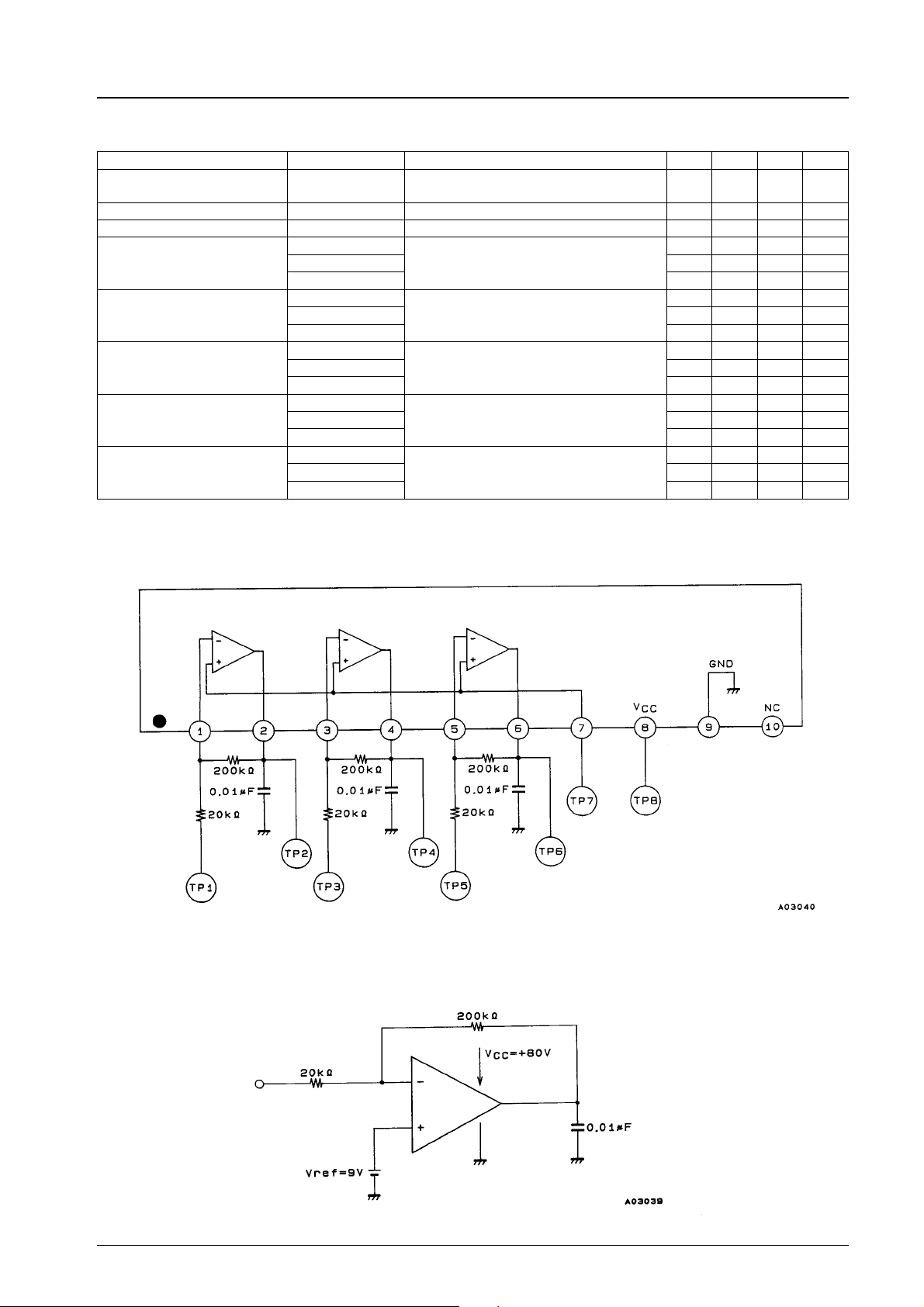
Internal Equivalent Circuit Block Diagram
When 6 V DC is applied to TP1, TP3 and
TP5, and 9 V is applied to TP7
When 12 V DC is applied to TP1, TP3 and
TP5, and 9 V is applied to TP7
When 0 V DC is applied to TP1, TP3 and
TP5, and 9 V is applied to TP7
When 3 V DC is applied to TP1, TP3 and
TP5, and 9 V is applied to TP7
When 6 V DC is applied to TP1, TP3 and
TP5, and 9 V is applied to TP7
When 9 V DC is applied to TP1, TP3 and
TP5, and 9 V is applied to TP7
1.9 2.2 2.7 mA
0.3 V
77 V
67 69 71 V
37 39 41 V
7911V
Test Circuit
No. 4957-2/3
 Loading...