Ordering number: EN5149B
Monolithic Linear IC
LA7846N
Vertical Deflection Output Circuit
Overview
The LA7846N is a vertical deflection output IC for TVs and
CRT displays with excellent image quality that use a BUS
control system signal processing IC. This IC can drive the
direct (even including a DC component) deflection yoke with
the sawtooth wave output from the BUS control system signal
processing IC. When used in conjunction with Sanyo’s LA7615
series of BUS control system signal processing ICs for TVs,
this IC can process all color television signal system functions
through the BUS system. Because the maximum deflection
current is 3.0 Ap-p, the LA7846N is suited for large screen
sets, being capable of driving screens ranging from 33 inches
to 37 inches.
Features
.
Low power dissipation due to built-in pump-up circuit
.
Vertical output circuit
.
Thermal protection circuit built in
.
Excellent crossover characteristics
.
DC coupling possible
Specifications
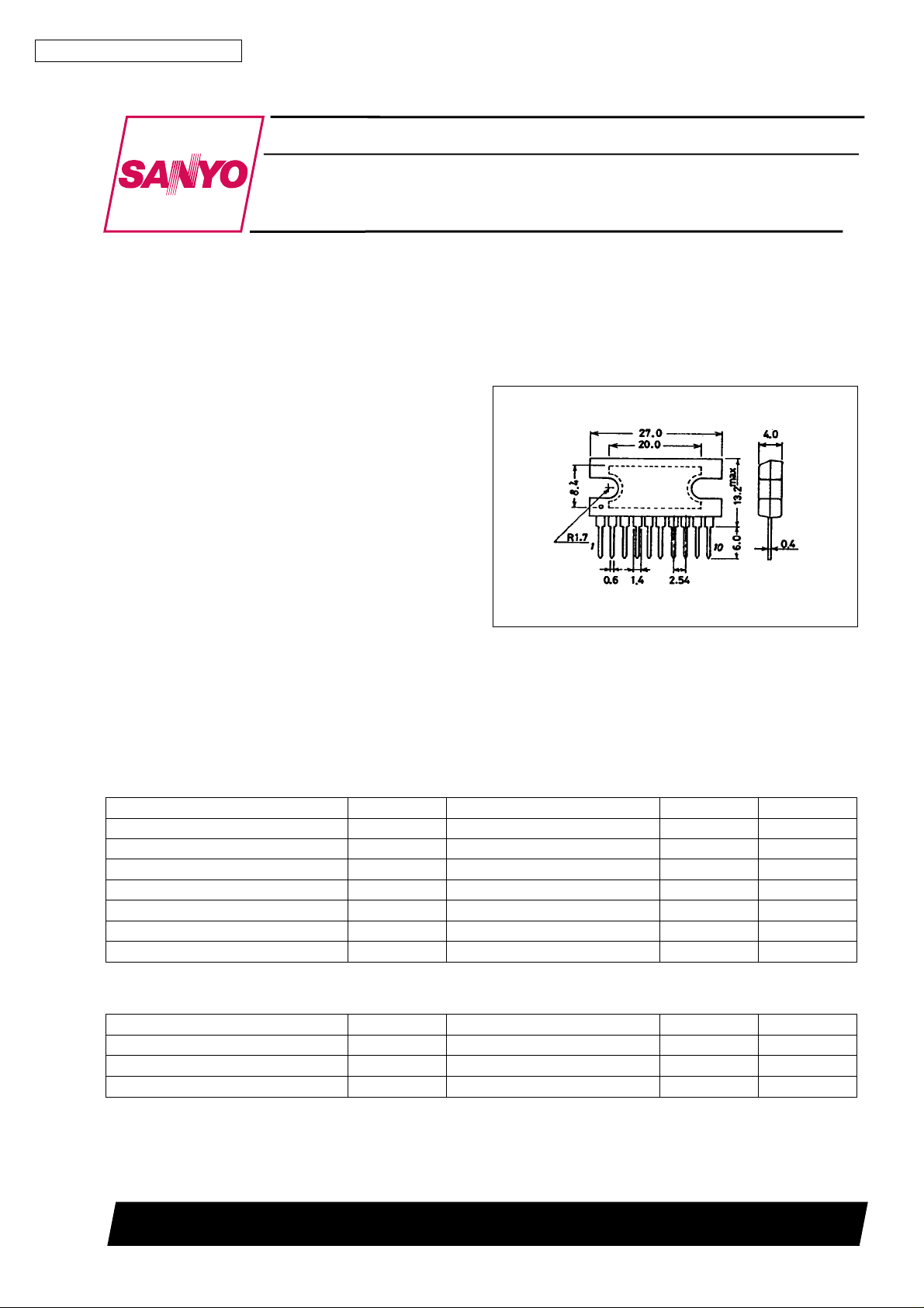
Package Dimensions
unit : mm
3024A-SIP10H
[LA7846N]
SANYO : SIP10H
Maximum Ratings atTa=25°C
Parameter Symbol Conditions Ratings Unit
Maximum supply voltage V
Output block supply voltage V
Deflection output current I 3 max –1.9 to +1.9 Ap-o
Thermal resistance θj-c 3.0
Allowable power dissipation Pd max With arbitrarily large heat sink fins 20 W
Operating temperature Topr –20 to +85
Storage temperature Tstg –40 to +150
7 max 40 V
CC
4 max 85 V
CC
Operating Conditions atTa=25°C
Parameter Symbol Conditions Ratings Unit
Recommended supply voltage V
Operating supply voltage range V
Recommended deflection output current I 3 p-p to 3.0 Ap-p
724V
CC
7op 16to38 V
CC
SANYO Electric Co.,Ltd. Semiconductor Bussiness Headquarters
TOKYO OFFICE Tokyo Bldg., 1-10, 1 Chome, Ueno, Taito-ku, TOKYO, 110 JAPAN
D1096HA(II)/N3095HA(II)/61595HA(II) No.5149-1/4
C/W
°
C
°
C
°

LA7846N
Operating Characteristics atTa=25°C, VCC7=24V
Parameter Symbol Conditions min typ max Unit
Pump-up charge saturation
voltage
Pump-up discharge saturation
voltage
Deflection output saturation
voltage (lower)
Deflection output saturation
voltage (upper)
Idling current I
Midpoint voltage V
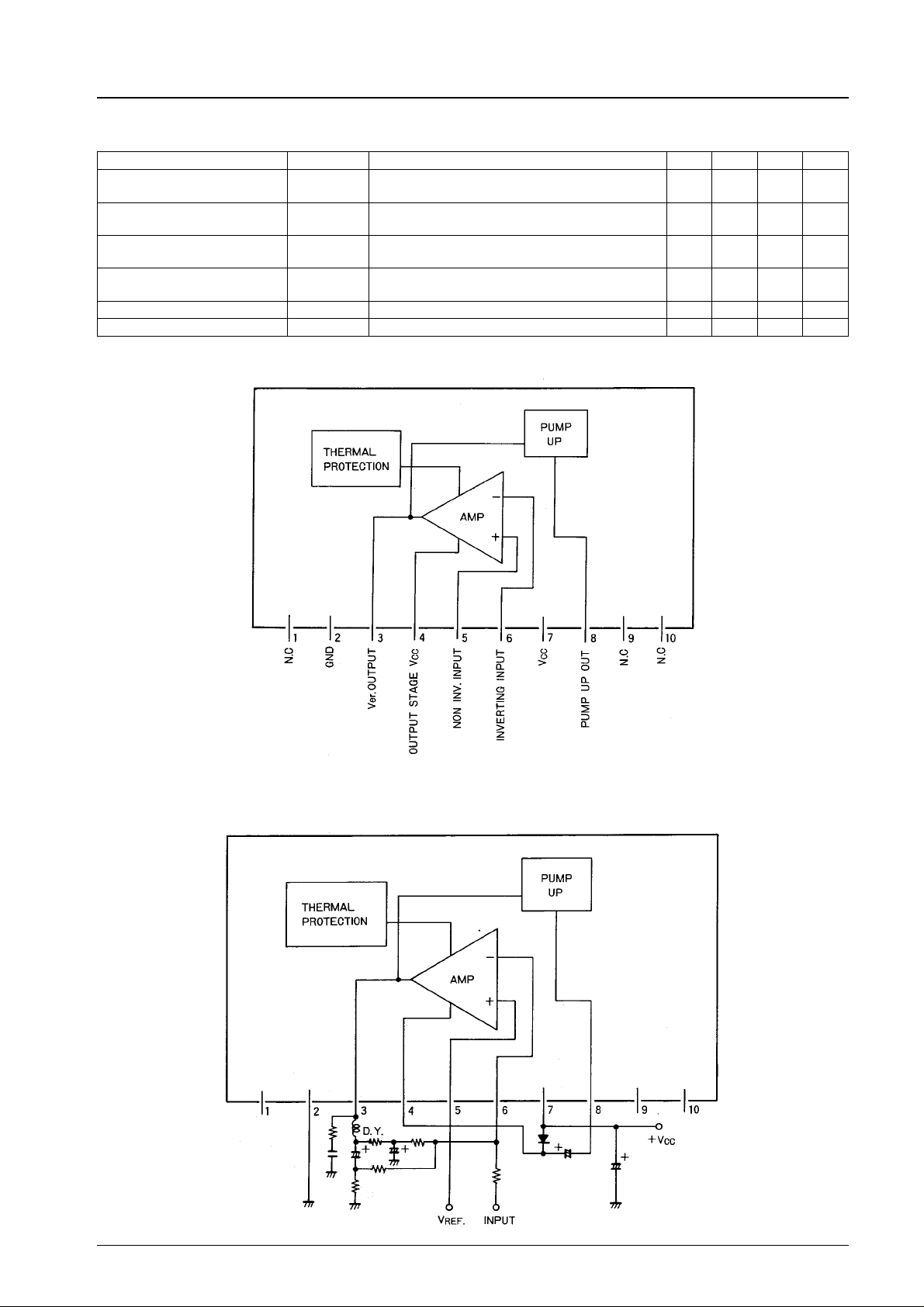
Block Diagram
V
8-2 I8=20mA 1.8 V
S
V
7-8 I 8 = –1.5 A 3.7 V
S
V
3-2 I 3 = 1.5 A 1.7 V
S
V
4-3 I 3 = –1.5 A 3.9 V
S
DL
MID
35 70 mA
11.0 12.0 13.0 V
Sample Application Circuit
(Single power supply)
No.5149-2/4
 Loading...