Page 1

Any and all SANYO products described or contained herein do not have specifications that can handle
applications that require extremely high levels of reliability, such as life-support systems, aircraft’s
control systems, or other applications whose failure can be reasonably expected to result in serious
physical and/or material damage. Consult with your SANYO representative nearest you before using
any SANYO products described or contained herein in such applications.
SANYO assumes no responsibility for equipment failures that result from using products at values that
exceed, even momentarily, rated values (such as maximum ratings, operating condition ranges,or other
parameters) listed in products specifications of any and all SANYO products described or contained
herein.
Monolithic Linear IC
Vertical Deflection Circuit
with TV/CRT Display Drive
Ordering number:ENN3313C
LA7837, 7838
SANYO Electric Co.,Ltd. Semiconductor Company
TOKYO OFFICE Tokyo Bldg., 1-10, 1 Chome, Ueno, Taito-ku, TOKYO, 110-8534 JAPAN
Overview
The LA7837, 7838 are vertical deflection output ICs developed for use in high-grade TVs and displays. The inter lace and crossover distortion responses, in particular, have
been greatly improved, allowing excellent picture quality
on large size televisions and high precision interlace mode
displays.
Also, pulse signals can be used for input signals due to the
on-chip sawtooth wave generating circuit and driver circuit. Further, the DC and A C feedback circuit can be formed
with these ICs alone, simplifying pattern design of sets and
ensuring stable performance. All of the functions in a color
TV signal system can be processed by connecting these
ICs with SANYO’s single-chip IC LA7670 series (NTSC)
and LA7680/85 series (PAL/NTSC) (VIF/SIF, video,
chroma, deflection).
The LA7837 has a maximum deflection current of 1.8App, making it appropriate for use in portable to mid-size televisions.
The LA7838 has a miximum deflection current of 2.2App, so it can be used for large size sets, and can drive from
33 to 37 inches.
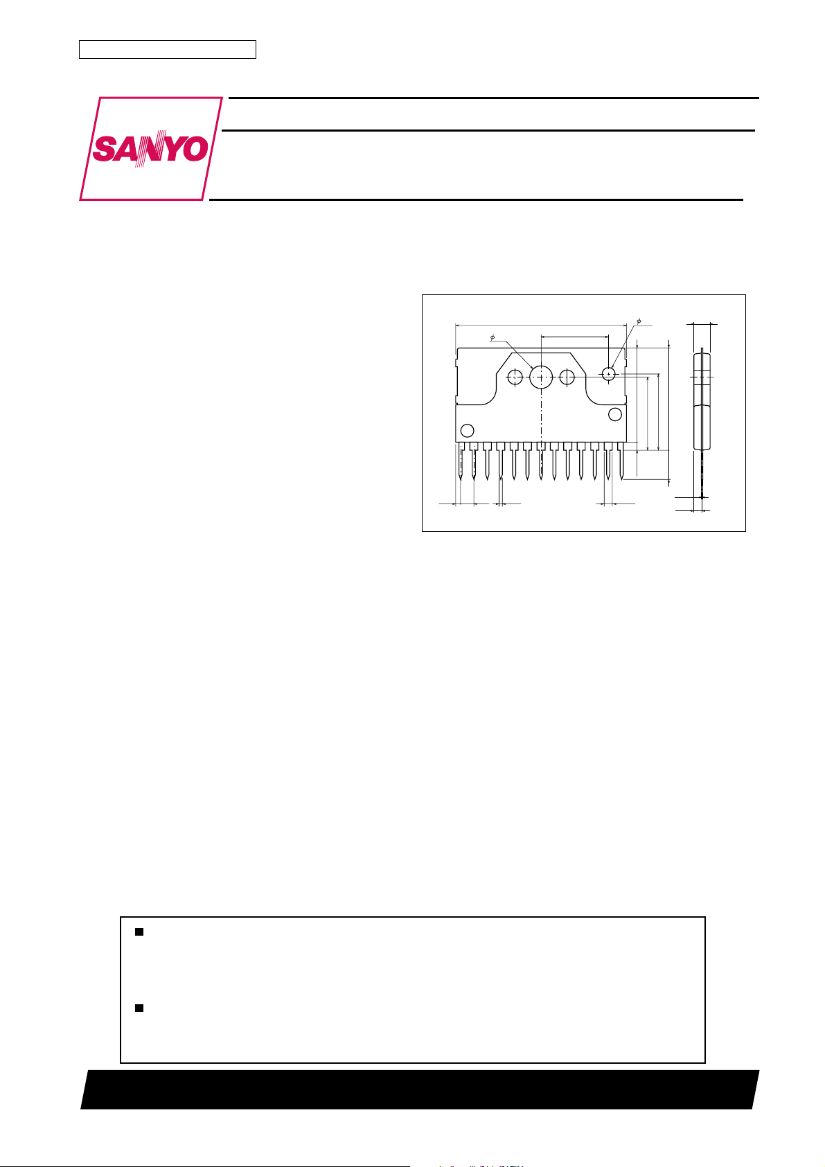
Package Dimensions
unit:mm
3107-SIP13H
[LA7837, 7838]
25.6
3.4
1
2.00.8
0.5
10.0
2.0
13.9
11.2
1.0min
13
1.15
SANYO : SIP13H
11.8
2.4
15.4max
4.5
0.4
1.2
Features
• Low power dissipation due to on-chip pump-up circuit.
• On-chip 50/60Hz vertical size control circuit.
• On-chip sawtooth wave generating circuit.
• On-chip driver circuit.
• Vertical output circuit.
• On-chip thermal protection circuit.
• Excellent interlace response.
• Excellent crossover response.
12501TN (KT)/71693TS/8251TS(KOTO)/2090TA, TS(AF) No.3313–1/9
Page 2

LA7837, 7838
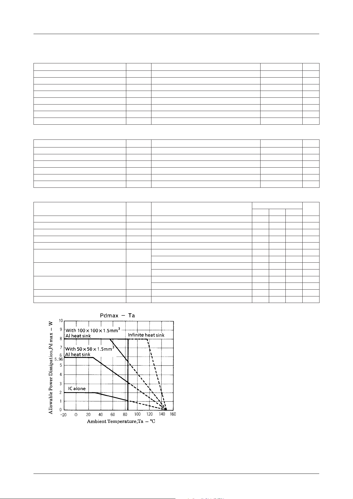
Specifications
Maximum Ratings at Ta = 25˚C
retemaraPlobmySsnoitidnoCsgnitaRtinU
V+
egatlovylppusrevirD
egatlovylppuspu-pmuP
egatlovylppustuptuO
tnerructuptuonoitcelfeDI
ecnatsiserlamrehT
noitapissidrewopelbawollAxamdPknistaehetinifnihtiW 8W
erutarepmetgnitarepOrpoT 58+ot02–
erutarepmetegarotSgtsT 051+ot04–
Operating Conditions at Ta = 25˚C, parenthesis ( ) indicates LA7838.
retemaraPlobmySsnoitidnoCsgnitaRtinU
egatlovylppusrevirddednemmoceRV+CC1 21V
egatlovylppusrevirdgnitarepOV+CC1 41ot8V
egatlovylppuspu-pmupdednemmoceRV+CC8 42V
egatlovylppuspu-pmupgnitarepOV+CC8 72ot01V
tnerructuptuonoitcelfeDp-p21I )2.2(8.1otpup-pA
thgieheslupmrofevawpmargnitarepOp-p6V }0.1–)3/1B+({otpup-pV
Operating Characteristics at Ta = 25˚C, +VCC1=12V, +VCC8=24V, parenthesis ( ) indicate LA7838.
retemaraPlobmySsnoitidnoC
tnerrucylppusrevirDI
egatlovdlohserhttupnireggirT2V6.29.22.3V
egatlovniplortnocedutilpmalacitreV4V9.51.63.6V
egatlovtratsnoitareneGmrofevawpmaRV
egatlovnoitarutasegrahcpu-pmuP11-9sVAm02=9I 8.1V
egatlovnoitarutasegrahcsidpu-pmuP9-8sV
)rewol(egatlovnoitarutastuptuonoitcelfeD11-21sV
)reppu(egatlovnoitarutastuptuonoitcelfeD21-31sV
tnerrucgnildII
niagegatloV 95Bd
xam1
CC
V+
xam8
CC
V+
xam31
CC
FED
θ c-j
sgnitaR
nimpytxam
16.57.68.7Am
CC
PMAR
A9.0=9I 0.3V
)A1.1=9I( )2.3(V
A9.0=21I 2.1V
)A1.1=21I( )5.1(V
A9.0=21I 2.3V
)A1.1=21I( )5.3(V
LD
6.49.42.5V
5356Am
51V
03V
26V
5.1+ot5.1–o-pA
˚C/W
4
˚C
˚C
tinU
No.3313–2/9
Page 3

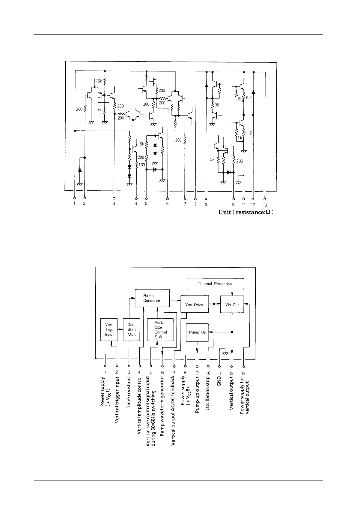
LA7837, 7838 Interface Circuit
LA7837, 7838
LA7837, 7838 Pin Connection Diagram and Block Diagram
No.3313–3/9
Page 4

LA7837, 7838
Sample Application Circuits for 14” Color TV
Fig. 1 +VCC1, 12V
Fig. 2 +VCC1, 9V
No.3313–4/9
Page 5

LA7837, 7838
Sample Application Circuits for 14” Display (Retrace Time≈300µs)
Change VR4 to fixed constant after adjustment.
( ) : For negative polarity pulse.
Fig. 3
No.3313–5/9
Page 6

LA7837, 7838
Precautions when using with display having short retrace time :
The vertical output ICs LA7837, 7838 are appropriate for use in monitors and displays because the interlace and
crossover distortion responses are superior to those of the LA7835, 7836.
However, since the vertical retrace time of displays is shorter than that of TV, the upper portion of the vertical
picture may stretch. This is because the start waveform of the pin 6 sawtooth wave bends, as shown in Fig.4, due to
the diode response of the clamp waveform. If there is not much time difference between T1 ant TR, the upper portion
of the vertical picture will tend to stretch. The use of a circuit as shown in Fig.3 will cause pin 6 waveform start
wave to become linear, so that stretching is suppressed. The example of circuit application shown in Fig.3 does not
use the trigger input circuit (pin 2) and one-shot multivibrator (pin 3) built in the LA7837, 7838 ; the pin 6 sawtooth
wave is controlled by the LA7855, 7856 vertical output pulse.
Therefore, the discharge circuit and clamp circuit are formed by the external Zener diode and transistor TR2.
Fig. 4
Design Example
For 12V pin 1 power supply
On the LA7837, 7838, pin 3 one-shot multivibrator operates when a trigger pulse enters pin 2. During this time, the
sawtooth wave generator discharge circuit and clamp circuit inside pin 6 operate.
The clamp voltage at this time is figured according to this formula :
V
CLAMP
=5/12 · V
........................... ¡
CC
For 12V,
V
CLAMP
=5 [V]
Therefore, the Zener diode used in Fig.3 must be rated more than 5V (e.g. 5.6V), otherwise the clamp circuit inside
the IC will operate.
For 9V pin 1 power supply
The same as for 12V, according to formula ¡ :
V
CLAMP
=3.75 [V]
So, that Zener diode must be rated more than 4V (e.g. 4.5V).
No.3313–6/9
Page 7

LA7837, 7838
Fig. 5
Pin 6 waveform when using the LA7837, 7838 in a display application circuit (Fig. 3)
Fig. 6
Fig. 7
No.3313–7/9
Page 8

LA7837, 7838
LA7837, 7838 application in a multi-sync system
The LA7837, 7838 can also be used in a vertical frequency multi-sync system.
The LA7837, 7838 do not have an on-chip vertical oscillation circuit, so they operate merely by impressing a trigger
pulse (e.g. 40 to 80Hz) on pin 2.
However, there are two problems with using the LA7837, 7838 as are in a multi-sync system.
One is vertical amplitude. When the trigger pulse changes between 40 to 80Hz, the vertical frequency will rise and
amplitude size decreases (because pin 6 cycle (T1, T2) in the diagram below becomes shorter).
Fig. 8
Countermeasure 1
In order to stabilize vertical size change, an
operational amplifier is used to change the
circuit to one which controls pin 4 vertical
size control current.
Voltage which corresponds to vertical frequency changes is applied to the operational
amplifier to stabilize vertical size.
The other problem is that vertical linearity chages when used at multi-frequency (e.g. 40 to 80Hz).
The reason for this is that R5 and C1 time constants are used for linearity correction (Fig.9), so even though the value
is optimum for a certain frequency, it is not for others.
Countermeasure 2
As shown in Fig.10, good linearity can be obtained by setting frequency ranges of use for R5 and C1 time constants for
vertical linearity correction, and switching them.
For example :
40 to 60Hz Switch A
60 to 80Hz Switch B
For switch A, R5 and C1 are set so that vertical linearity response is optimum for fv≈50Hz.
Next, for switch B, R5’ and C1’ are set for optimum value at fv≈70Hz.
By dividing the vertical trigger pulse range (e.g.40 to 80Hz) and performing linearity correction in this way, linearity
distortion can be kept below about 3%.
No.3313–8/9
Page 9

LA7837, 7838
Reference
For example, when using the LA7837, 7838 on a multi-sync system with 40 to 80Hz vertical frequency, vertical
linearity distortion will be less than approximately 4%, if vertical size is always uniform.
Therefore, if linearity response of better than 4% is desired, the linearity correnction time constant switching circuit
shown is Fig.10 should be used.
Fig. 10
Specifications of any and all SANYO products described or contained herein stipulate the performance,
characteristics, and functions of the described products in the independent state, and are not guarantees
of the performance, characteristics, and functions of the described products as mounted in the customer's
products or equipment. To verify symptoms and states that cannot be evaluated in an independent device,
the customer should always evaluate and test devices mounted in the customer's products or equipment.
SANYO Electric Co., Ltd. strives to supply high-quality high-reliability products. However, any and all
semiconductor products fail with some probability. It is possible that these probabilistic failures could
give rise to accidents or events that could endanger human lives, that could give rise to smoke or fire,
or that could cause damage to other property. When designing equipment, adopt safety measures so
that these kinds of accidents or events cannot occur. Such measures include but are not limited to protective
circuits and error prevention circuits for safe design, redundant design, and structural design.
In the event that any or all SANYO products(including technical data,services) described or
contained herein are controlled under any of applicable local export control laws and regulations,
such products must not be exported without obtaining the export license from the authorities
concerned in accordance with the above law.
No part of this publication may be reproduced or transmitted in any form or by any means, electronic or
mechanical, including photocopying and recording, or any information storage or retrieval system,
or otherwise, without the prior written permission of SANYO Electric Co. , Ltd.
Any and all information described or contained herein are subject to change without notice due to
product/technology improvement, etc. When designing equipment, refer to the "Delivery Specification"
for the SANYO product that you intend to use.
Information (including circuit diagrams and circuit parameters) herein is for example only ; it is not
guaranteed for volume production. SANYO believes information herein is accurate and reliable, but
no guarantees are made or implied regarding its use or any infringements of intellectual property rights
or other rights of third parties.
This catalog provides information as of January, 2001. Specifications and information herein are subject
to change without notice.
PS No.3313–9/9
 Loading...