

Any and all SANYO products described or contained herein do not have specifications that can handle
applications that require extremely high levels of reliability, such as life-support systems, aircraft’s
control systems, or other applications whose failure can be reasonably expected to result in serious
physical and/or material damage. Consult with your SANYO representative nearest you before using
any SANYO products described or contained herein in such applications.
SANYO assumes no responsibility for equipment failures that result from using products at values that
exceed, even momentarily, rated values (such as maximum ratings, operating condition ranges, or other
parameters) listed in products specifications of any and all SANYO products described or contained
herein.
Overview
The LA7780M is a downconverter for QPSK data
demodulation for digital CATV transmission. This IC
integrates a preamplifier, an AGC amplifier, a mixer, an
oscillator, a post-amplifier, and other circuits in a single
chip, and provides all the functions required from cable
signal input through output to the A/D converter.
Features
• Since a preamplifier is built in, the LA7780M has
adequate sensitivity to handle the input signal from the
cable directly.
(Input signal level:–30 to +30 dBm)
• Both internal and external AGC are supported as the
AGC amplifier drive technique.
• The output amplitude of the post amplifier used to drive
the A/D converter is 2 Vp-p (typical).
• Applications can be designed to use either a crystal or an
inductor oscillator.
Functions
• Preamplifier
• AGC amplifier
• Mixer
• Oscillator
• Post amplifier
• IF AGC (internal/external)
• AGC detector
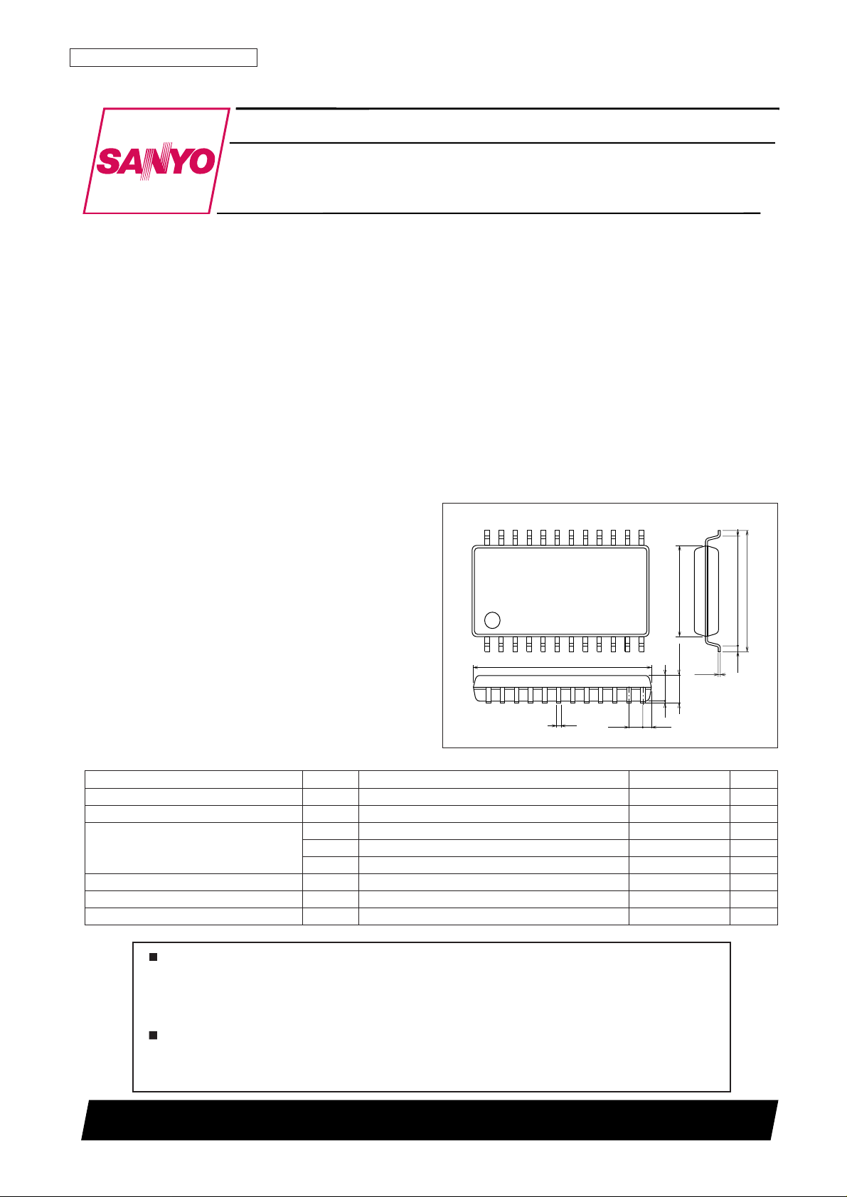
Package Dimensions
unit: mm
3108-MFP24D
0.25
24
13
15.3
112
0.67
0.4
1.27
7.9
9.2
10.5
0.625
2.55max
2.250.1
Monolithic Linear IC
D1698RM (OT) No. 5268-1/9
SANYO: MFP24D
[LA7780M]
SANYO Electric Co.,Ltd. Semiconductor Bussiness Headquarters
TOKYO OFFICE Tokyo Bldg., 1-10, 1 Chome, Ueno, Taito-ku, TOKYO, 110-8534 JAPAN
QPSK Downconverter for CATV Systems
LA7780M
Ordering number : EN5268A
Parameter Symbol Conditions Ratings Unit
Maximum supply voltage V
CC
max Pins 5, 6, and 17 7.0 V
Circuit voltage V max Pins 4, 12, and 24 V
CC
V
I
4
The pin 4 output current 30 mA
Circuit current I
13
The pin 13 sink current 2 mA
I
16
The pin 16 sink current 2 mA
Allowable power dissipation Pd max Ta ≤ 70°C 540 mW
Operating temperature Topr –20 to +70 °C
Storage temperature Tstg –55 to +150 °C
Specifications
Maximum Ratings at Ta = 25°C
No. 5268-2/9
LA7780M
Parameter Symbol Conditions
Ratings
Unit
min typ max
Circuit current I
total
Pins 4, 5, 6, and 17: no signal 64 80 95 mA
RF input frequency range f
(in)
Pins 1, 8, and 9 30 150 MHz
IF output level V
O(IF)
Pin 13: *1 1.6 2.0 2.5 Vp-p
IF output IM3 V
O(IM3)
Pin 13: *2 40 dB
IF output frequency bandwidth BW Pin 13: *3 15 MHz
Local oscillator frequency range f
(LO)
Pins 18, 19, 20, and 21 30 200 MHz
AGC amplifier input sensitivity Vin(RF2) Pins 8 and 9: *4 –25 –21 –17 dBmV
AGC range GR Pin 13: IF output level < ±1 dB 60 80 dB
AGC flatness ∆V
O(IF)
Pin 13: Compare with the state when
–1 0 +1 dB
Vin (RF2) = 30 dBmV
Preamplifier gain G
(RF1)
Pin 4: *5 17 19 21 dB
Maximum preamplifier output level V
Omax
Pin 4: *6 50 dBmV
Oscillator output level V
O(OSC)
Pin 23: The pin 23 frequency is 1/2 that of
500 800 1000 mVp-p
the local oscillator
AC Characteristics at Ta = 25°C, VCC= 5.0 V, internal AGC mode, Pin 24 is left open.
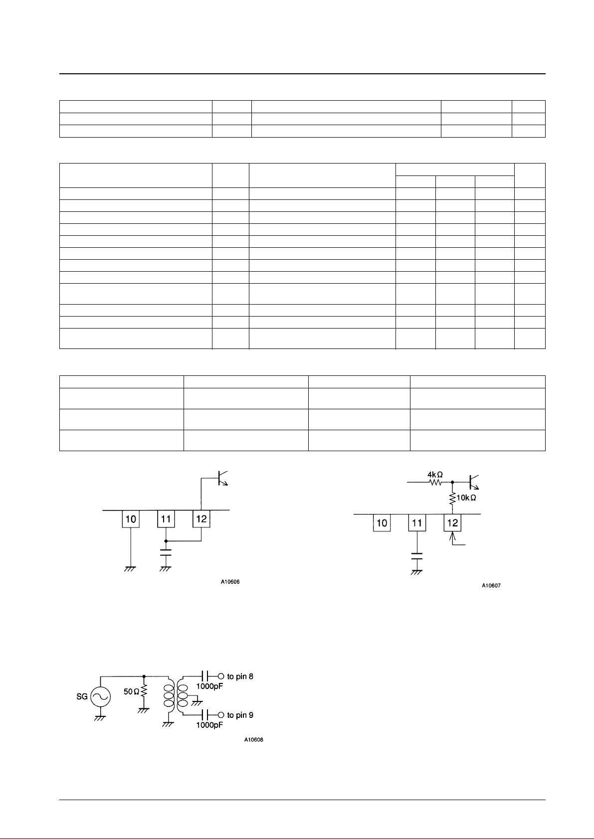
Operating Modes
Mode Pin 10 Pin 11 Pin 12
Internal AGC GND
With a capacitor between
Connected to pin 11
pin 11 and ground
External AGC GND With a capacitor between External AGC voltage supply
(Narrow control range: 3 to 5 V) (AGC divider inactive) pin 11 and ground Pin 12 = high impedance
External AGC Open With a capacitor between External AGC voltage supply
(Wide control range: 0 to 5 V) (AGC divider active) pin 11 and ground Pin 12 = low impedance (14 kΩ)
Internal AGC
External AGC
Caution:
Note 1.
Input: SG = 69.55 MHz, 20 dBm V
Other conditions:
Internal AGC mode
Pin 24 left open.
Output: The post amplifier output (pin 13) at 5 MHz
Note: In internal AGC mode, the IF output level can be adjusted by varying the pin 24 DC voltage.
Parameter Symbol Conditions Ratings Unit
Recommended supply voltage V
CC
Pins 5, 6, and 17 5.0 V
Operating supply voltage range V
CC
op Pins 5, 6, and 17 4.5 to 5.5 V
Operating Conditions at Ta = 25°C
Transfer ratio = 1 : 1
No. 5268-3/9
LA7780M
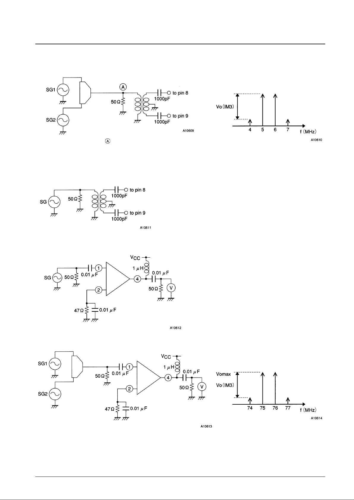
Note 2.
Input: SG1 = 69.55 MHz, SG2 = 70.55 MHz
Other conditions:
Internal AGC mode
Pin 24 left open.
Output: The post amplifier output (pin 13)
Note 3.
Post amplifier output level = –3 dB
Remove the low-pass filter between pins 14 and 16.
(
Short the coil of 27 µH and remove the capacitors of 27 pF and 15 pF.)
Note 4.
Input: SG1 = 69.55 MHz
Note 5.
SG = 75 MHz, 20 dBm V
Note 6.
SG1 = 75 MHz, SG2 = 76 MHz,
Adjust the pin 1 level until the IM3 in the pin 4 output is 40 dB.
Output:RF1-OUT (pin 4)
V
O(IM3)
= 40 dB
Other conditions:
Internal AGC mode
Pin 24 left open.
Output: The signal level such that the post
amplifier output (pin 13) falls by –3 dB.
Point = 20 dBmV (69.55 MHz) + 20 dBmV (70.55 MHz)
 Loading...