

Page 1
Any and all SANYO products described or contained herein do not have specifications that can handle
applications that require extremely high levels of reliability, such as life-support systems, aircraft’s
control systems, or other applications whose failure can be reasonably expected to result in serious
physical and/or material damage. Consult with your SANYO representative nearest you before using
any SANYO products described or contained herein in such applications.
SANYO assumes no responsibility for equipment failures that result from using products at values that
exceed, even momentarily, rated values (such as maximum ratings, operating condition ranges,or other
parameters) listed in products specifications of any and all SANYO products described or contained
herein.
Monolithic Linear IC
FSK Receiver for CATV Use
Ordering number:ENN2208A
LA7770
SANYO Electric Co.,Ltd. Semiconductor Company
TOKYO OFFICE Tokyo Bldg., 1-10, 1 Chome, Ueno, Taito-ku, TOKYO, 110-8534 JAPAN
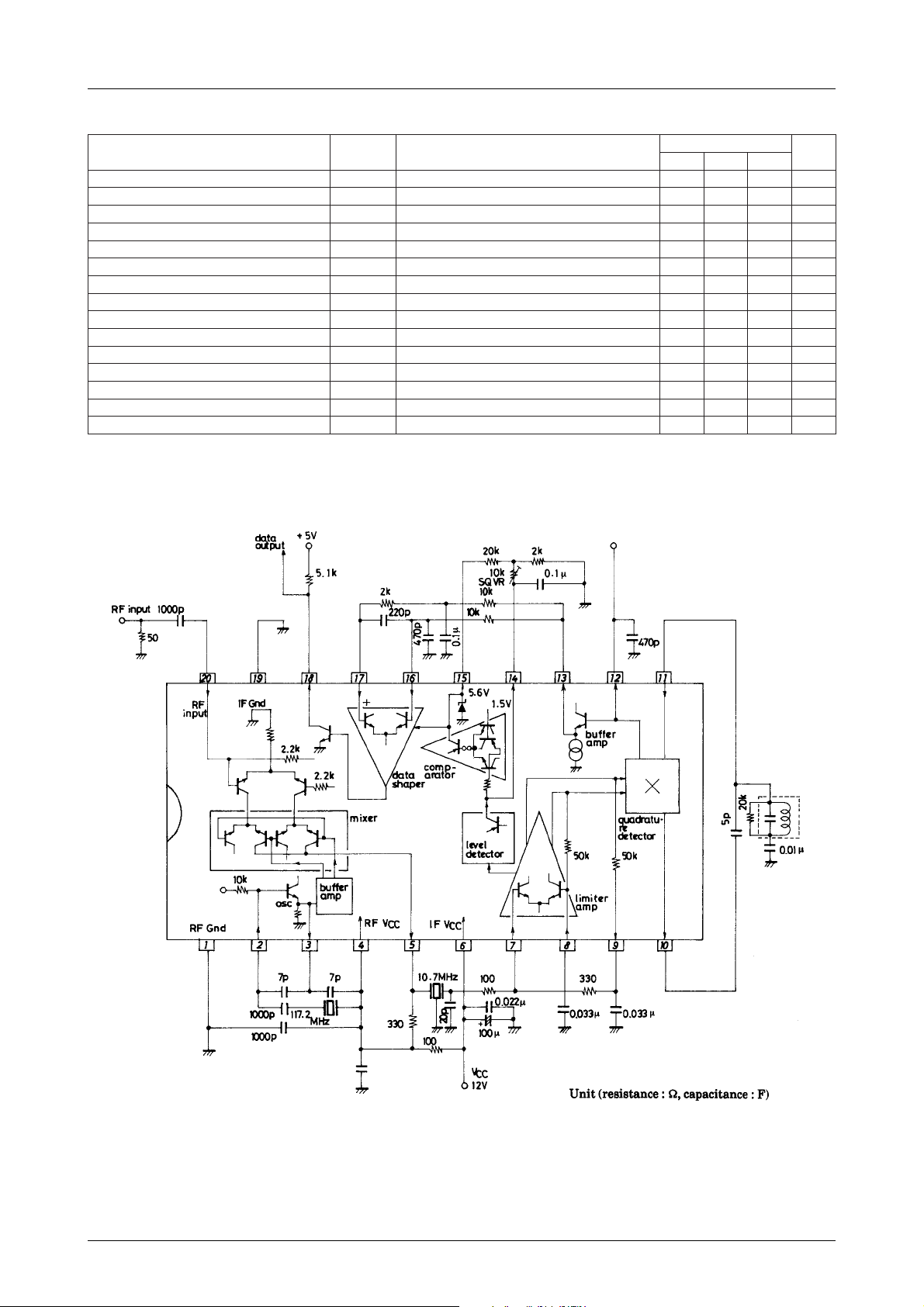
Overview
The LA7770 is a CATV-oriented wide-band FSK (frequency shift keying) receiv er IC encapsulated in a DIP20S
package that incorporates the functions required to demodulate scramble decoding data (i. e., the oscillator, mixer, lim-
iting IF amplifier, squelcher, and data shaper functions).
Features
• High limiting sensitivity.
• Incorporating a common-collector oscillator enables LC,
crystal, or SAW-R (surface acoustic wave resonator) operated oscillations, as required by application.
Functions
• Mixer.
• Limiting IF amplifier.
• Squelch meter drive.
• Oscillator.
• Quadrature detector.
• Data shaper.
Specifications
Maximum Ratings at Ta = 25˚C
retemaraPlobmySsnoitidnoCsgnitaRtinU
egatlovylppusmumixaM
tnerructuo-wolfmumixaMI
noitapissidrewopelbawollAxamdP 077Wm
erutarepmetgnitarepOrpoT 58+ot02–
erutarepmetegarotSgtsT 521+ot55–
V
V
xam4 51V
CC
xam6 51V
CC
xam 3Am
81
Ta≤65˚C
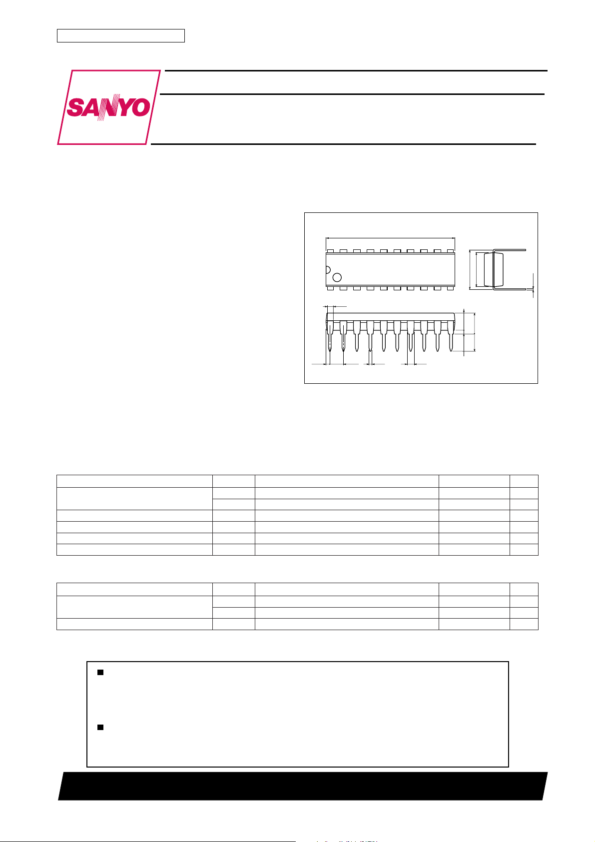
Package Dimensions
unit:mm
3021C-DIP20
[LA7770]
24.0
20
1
1.0
(0.57)
2.54
0.5
1.2
11
7.62
10
(3.25)
3.9max
3.3
0.51min
SANYO : DIP20
6.4
0.25
˚C
˚C
Operating Conditions at Ta = 25˚C
retemaraPlobmySsnoitidnoCsgnitaRtinU
egnaregatlovgnitarepO
egnaregatlovtupnirotarapmoC91V,61V V(otV2
VCC4 21ot9V
VCC6 21ot9V
13101TN (KT)/O0695TH (KOTO)/D088MO/O127TA, TS No.2208–1/7
)V2–V
CC
Page 2
LA7770
Operating Characteristics at Ta = 25˚C
retemaraPlobmySsnoitidnoC
tnerructnecseiuQoccIffo-QS229273Am
tnerructiucriCI
ecnaticapactupnirexiMiczHM0017Fp
ecnatsisertupnirexiMirzHM001086
niagegatlovrexiMmgVRL003= Ω M5.601, → M7.0192151Bd
ytivitisnesgnitimilBd3–iV
N/SN/S
noitrotsidcinomrahlatoTDHT
tuptuonoitaludomeDoV
noitcejerMARMAzHk1ta%03:MA7455Bd
evirdreteMI
egatlovdlohserhthcleuqSV
tnerructupnirepahsataDI
egatlovnoitarutastuptuOV
ytuD|DT|zHk41=f5.20.5%
CC
D
HT41
61
no-QS0.325.030.93Am
∆
F
∆
F
∆
F
∆
F
Aµ003 → Aµ00652102Bd/Aµ
CD8.05.12.2V
CD7.00.3Aµ
I
)tas(81
Am2=1.07.0V
81
zHk1ta,vedzHk57±=
zHk1ta,vedzHk57±=
zHk1ta,vedzHk57±=
zHk1ta,vedzHk57±=
nimpytxam
Equivalent Circuit Block Diagram
sgnitaR
5213Vµ/Bd
7455Bd
6.02%
003044006smrVm
tinU
Ω
No.2208–2/7
Page 3
LA7770
LA7770 Dynamic Behavior and Cautions on Designing
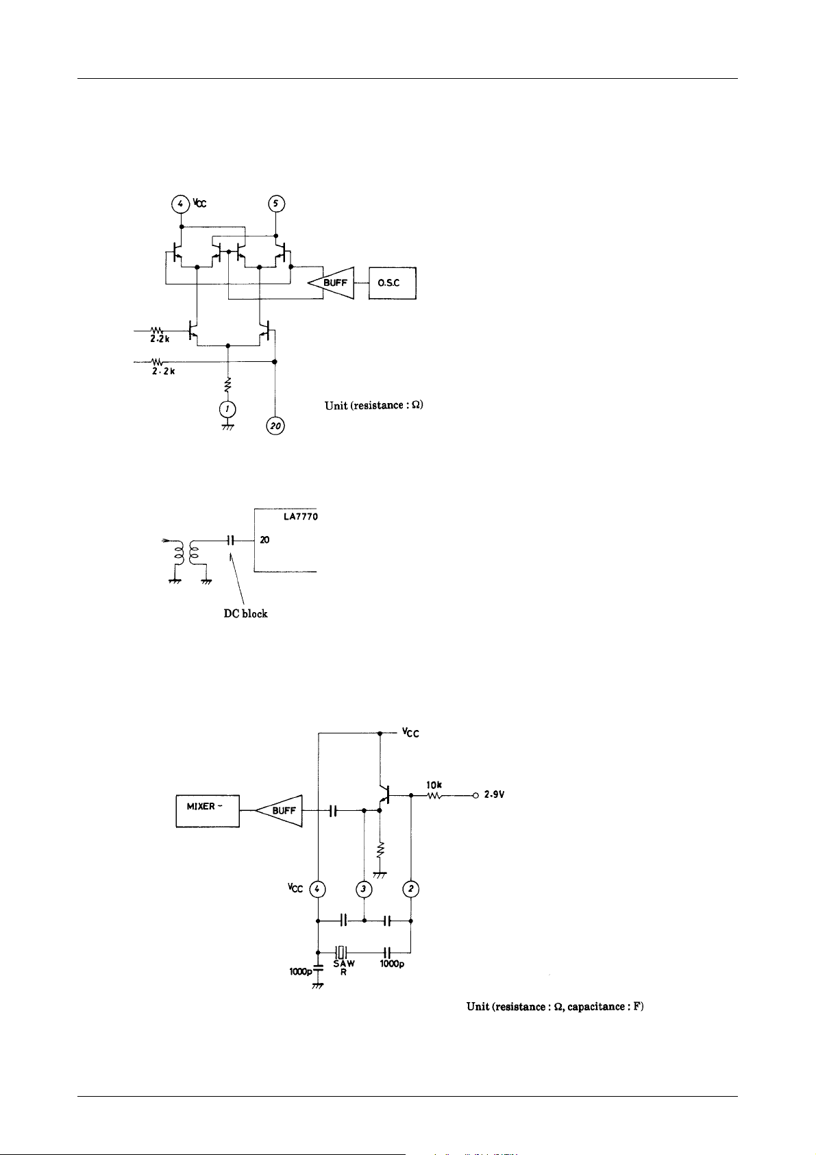
(1) Mixer
A double differential type mixer is employd with its input circuit configured as shown in Fig. 1, where the input
signal is mixed with the oscillator output by its double differential circuit.
The mixed signal will be output from its open collector pin 5.
Fig. 1
Caution
a. Since an internal bias is applied to the input pin (pin 20), be
sure to provide a DC blocking capacitor as shown in Fig. 2.
b. Connect the decoupling capacitor across pins 4 and 1 with the
shortest possible wiring.
Fig. 2
(2) Oscillator
A common-collector oscillator is employed as shown in Fig. 3, and enables the LC, crystal, or SAW-R operated
oscillations.
Fig. 3
No.2208–3/7
Page 4

LA7770
(3) IF Limiting Amplifier
The limiter amplifier employed is made up of DC feedback-provided 6-stage direct-coupled differential amplifiers.
Simplified, its circuit is represented in Fig. 4 below.
Fig. 4
Feedback gain (AV) will be AV= = ≈
where feedback depth β = =
V2
V1
A
1+Aβ
√1+ (ωCR)
1
1
+β
A
1
β
1
2
so that the decoupling capacitor C should be made sufficiently
large in capacitance within the operating frequency band to
achieve its low impedance.
(4) Quadrature Detector
The quadrature detector converts a frequency-modulated signal into a phase-modulated one by passing it through a
phase shifter, and then demodulates it by converting it again into voltage with its phase detector.
The quadrature detector block of the LA7770 is configured as shown in Fig. 5 below.
Fig. 5
Phase Shifter
The phase shifter is an important element of the quadrature detector, and it dictates the detection characteristics of
the latter.
The following phase-shifter-related parameters may be cited.
1. Demodulation output ...........Chiefly QL
2. Distortion Factor.................. Phase shifter linearity and symmetry of S curve
* While the phase shifting linearity may be enhanced with a single tuning circuit by lowering its QL and broaden-
ing its frequency band, its demodulation output will also be lowered in the process.
Fig. 6
No.2208–4/7
Page 5

LA7770
In the Fig. 6 phase shifter,
1
V2
==
V1
Requirements to achieve a 90° phase shift will be :
jωC2+ +jwL
1
jωC1
1
R
+
jωC2+ +jwL
1
1
R
ω2L (C1+C2)–1
ω2LC1
1
1
–j
jωCR
ω2L (C1+C2)=1 ∴ƒ=
ω=
V2
V1
At the tuning point :
V2
V1
(5) Meter Drive and Squelch
A forward bias is provided to the meter drive dedicated detector, to enable its detector diode to detect low-level
signals. In addition, a bias canceler is also provided to eliminate the offsetting current in a no-signal mode created
by the forward bias. Furthermore, to broaden the linear operating range, signals are fetched from the 3rd and 5th
stage outputs of the limiter amplifier, for composition together after level detection.
1
√L (C1+C2)
=
ω2L (C1+C2)–1
√
=
ωC1R
√
ω2LC1
1
1
1
=ωC1R
2
1
2π√L (C1+C2)
2
1
+
jωC1R
2
Fig. 7
No.2208–5/7
Page 6

LA7770
The composite current after the level detection flows out from pin 14, and after its being converted to a voltage by
an externally connected circuit, will detremine V1 of the comparator.
The squelch circuit may be provided with hysteresis by providing a resistor feedback from pin 15 to pin 14.
Fig. 8
(6) Data Shaper
The data shaper is a high-impedance input differential amplifier that provides an open-collector output. It serves to
facilitate the design for matching with a following stage (such as a CPU).
Fig. 9
No.2208–6/7
Page 7

LA7770
Specifications of any and all SANYO products described or contained herein stipulate the performance,
characteristics, and functions of the described products in the independent state, and are not guarantees
of the performance, characteristics, and functions of the described products as mounted in the customer's
products or equipment. To verify symptoms and states that cannot be evaluated in an independent device,
the customer should always evaluate and test devices mounted in the customer's products or equipment.
SANYO Electric Co., Ltd. strives to supply high-quality high-reliability products. However, any and all
semiconductor products fail with some probability. It is possible that these probabilistic failures could
give rise to accidents or events that could endanger human lives, that could give rise to smoke or fire,
or that could cause damage to other property. When designing equipment, adopt safety measures so
that these kinds of accidents or events cannot occur. Such measures include but are not limited to protective
circuits and error prevention circuits for safe design, redundant design, and structural design.
In the event that any or all SANYO products(including technical data,services) described or
contained herein are controlled under any of applicable local export control laws and regulations,
such products must not be exported without obtaining the export license from the authorities
concerned in accordance with the above law.
No part of this publication may be reproduced or transmitted in any form or by any means, electronic or
mechanical, including photocopying and recording, or any information storage or retrieval system,
or otherwise, without the prior written permission of SANYO Electric Co. , Ltd.
Any and all information described or contained herein are subject to change without notice due to
product/technology improvement, etc. When designing equipment, refer to the "Delivery Specification"
for the SANYO product that you intend to use.
Information (including circuit diagrams and circuit parameters) herein is for example only ; it is not
guaranteed for volume production. SANYO believes information herein is accurate and reliable, but
no guarantees are made or implied regarding its use or any infringements of intellectual property rights
or other rights of third parties.
This catalog provides information as of January, 2001. Specifications and information herein are subject
to change without notice.
PS No.2208–7/7
 Loading...