

Overview
The LA7688 integrates VIF, SIF, video, chrominance, and
deflection processing circuits for PAL/NTSC format TV
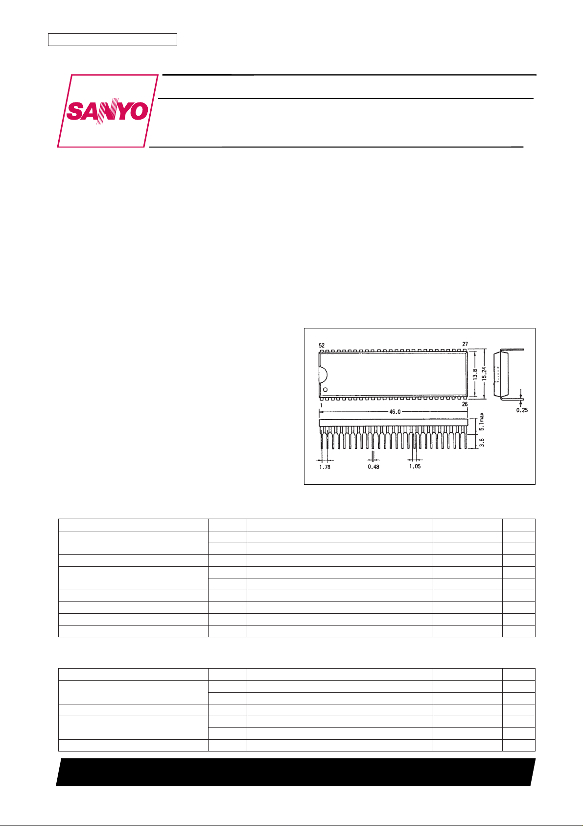
sets on a single chip and is provided in a 52-pin shrink
package.
The VIF and SIF circuits achieve semi-adjustment-free
operation, and are adjustment-free except for the VCO coil
and the RF AGC circuit. The chrominance circuit can be
made adjustment-free by using the LC89950 1H delay line
IC. All the signal processing required for a multi-format
color TV can be implemented by combining this product
with the LA7642 SECAM decoder IC.
Features
[VIF] • PLL detector • Buzz canceller
[SIF] • PLL detector • Audio switch
[VIDEO] • Built-in trap • Built-in DL
• Aperture control
• Video switch (SVO output)
• Black expansion
[CHROMA] • PAL/NT • Base band processing
(adjustment free)
• Built-in bandpass filter
[OSD] • Analog OSD
[DEF] • Automatic 50/60 Hz discrimination
• Fixed vertical size • Double AFC
• Built-in sync separator circuit
[Other features] • Sandcastle pulse (for the 1H delay line)
• fsc output (for SECAM systems)
• Primary color output
Package Dimensions
unit: mm
3218-DIP52S
Monolithic Linear IC
Ordering number : EN5635
82097HA(OT) No. 5635-1/6
SANYO: DIP52S
[LA7688]
SANYO Electric Co.,Ltd. Semiconductor Bussiness Headquarters
TOKYO OFFICE Tokyo Bldg., 1-10, 1 Chome, Ueno, Taito-ku, TOKYO, 110 JAPAN
Single-Chip CTV Signal-Processing Circuit
for PAL and NTSC Formats
LA7688
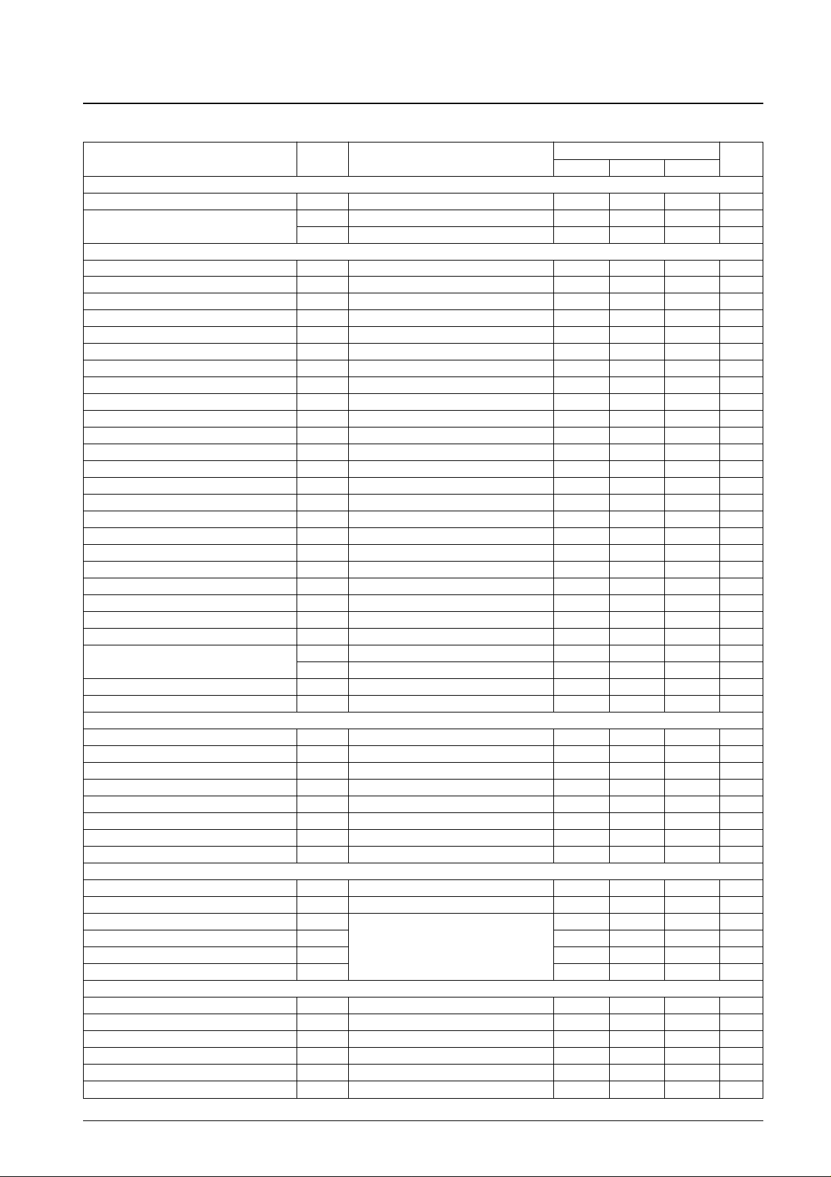
Parameter Symbol Conditions Ratings Unit
Maximum supply voltage
V
40
max 9V
V
45
max 9V
Maximum supply current I
24
max 16 mA
FBP input current
I
26
max 5mA
I
32
max 10 mA
FBP input voltage I
26
min –5 V
Allowable power dissipation Pd max Ta ≤ 65°C When mounted on a printed circuit board* 1.3 W
Operating temperature Topr –10 to +65 °C
Storage temperature Tstg –55 to +150 °C
Specifications
Maximum Ratings at Ta = 25°C
Parameter Symbol Conditions Ratings Unit
Recommended supply voltage
V
40
7.6 V
V
45
7.6 V
Recommended supply current I24 12 mA
Operating voltage range
V
40
op 7 to 8.2 V
V
45
op 7 to 8.2 V
Operating current range I
24
op 10 to 16 mA
Operating Conditions at Ta = 25°C
Note : * Printed circuit board size: 83 × 86 × 1.5 mm, material: Bakelite
No. 5635-2/6
LA7688
Parameter Symbol Conditions
Ratings
Unit
min typ max
[Circuit Voltages and Currents]
Horizontal power-supply voltage V
CC
H Deflection system (V24) 6.4 6.9 7.4 V
Current drain
I
40
78 90 100 mA
I
45
34 40 48 mA
[VIF Block]
RF AGC maximum voltage V
50H
7.5 7.8 7.8 V
RF AGC minimum voltage V
50L
0.2 0.6 V
Input sensitivity V
i
39 45 dBµ
AGC range GR 56 60 dB
Maximum allowable input V
IN max
95 100 dBµ
Quiescent video output voltage V
8
4.1 4.4 4.7 V
Synchronizing signal tip voltage V
8tip
1.7 2.0 2.3 V
Video output amplitude V
O
1.7 2.0 2.3 Vp-p
Black noise threshold voltage V
BTH
1.0 1.3 1.7 V
Black noise clamp voltage V
BCL
2.7 3.0 3.3 V
Output signal-to-noise ratio S/N 48 52 dB
1.07 MHz beat level C/S 40 44 dB
Frequency characteristics f
C
6 9 MHz
Differential gain DG 5 10 %
Differential phase DP 6 10 deg
Quiescent AFT voltage V
7
3.6 3.9 4.2 V
Maximum AFT voltage V
7H
7.3 7.6 7.8 V
Minimum AFT voltage V
7L
0 0.3 0.7 V
AFT detection sensitivity Sf 10 15 20 mV/kHz
VIF input resistance Ri f = 38.9 MHz 1.0 1.3 1.6 kΩ
VIF input capacitance Ci f = 38.9 MHz 2 3 5 pF
APC pull-in range (U) f
PU
0.8 2.0 MHz
APC pull-in range (L) f
PL
–2 –0.8 MHz
VCO1 maximum variation range
∆
fU1
0.8 2.0 MHz
∆
fL1
–2.0 –0.8 MHz
SIF signal level S
OUT
110 140 170 mVrms
VCO1 control sensitivity ß 2.4 4.8 9.6 kHz
[SIF Block]
SIF limiting sensitivity V
i
(lim) 40 46 52 dBµ
FM detector output voltage V
O
(FM) 390 500 710 mVrms
AMR AMR 40 60 dB
Total harmonic distortion THD 0.3 1.0 %
SIF S/N S/N (SIF) 55 62 dB
FM detector range (L) W
FML
2.5 4.0 MHz
FM detector range (H) W
FMH
7.0 8.0 MHz
FM detector output variability ∆V
O
0 2.0 3.0 dB
[INT/EXT Switching Block]
AFT EXT gain G
AF
–0.7 –0.2 +0.3 dB
AFT EXT distortion THD
AF
0.03 0.5 %
System switch I-SE V1
TH1
Notes: 0 1.2 V
System switch I-P/N V1
TH2
I = INT, E = EXT 1.7 2.6 V
System switch E-P/N V1
TH3
P/N = PAL/NTSC 2.9 3.8 V
System switch E-SE V1
TH4
SE = SECAM 4.1 5 V
[Video Switching Block]
Video signal input 1 DC voltage V
10DC
3.2 3.5 3.8 V
Video signal input 1 AC voltage V
10AC
1.0 Vp-p
Video signal input 2 DC voltage V
14DC
3.2 3.5 3.8 V
Video signal input 2 AC voltage V
14AC
1.0 Vp-p
SVO pin DC voltage V
16DC
2.5 2.8 3.1 V
SVO pin AC voltage V
16AC
1.7 2.0 2.3 Vp-p
Operating Characteristics at Ta = 25°C, V
CC40, 45
= 7.8 V, I24= 12 mA
Continued on next page.
 Loading...