

Sanyo LA7674 Specifications
Ordering number : ENN4361
71599RM (OT)/41893TS A8-9533 No. 4361-1/6
Overview
The LA7674 improves upon the black-level, horizontaljitter, switch-on drift performance of the single-chip
LA7672 used to date. Also a single-chip IC, the LA7674
is for color TVs based on the NTSC (National Television
System Committee) system with an on-chip circuit for all
VIF, SIF, video, chroma and deflection signal processing.
Functions and Features
[VIF]
• PLL detection (high video and audio quality)
• High-gain VIF amplifier
• High speed AGC
• On-chip APC time constant switch
[SIF]
• Simultaneous sound IN/OUT
• Video/audio simultaneous muting, or audio-only muting
possible
[Audio-visual switch]
• Internal/external audio-visual switch (VCC= 9V)
[OSD]
• RGB 3 input
• RGB linear amplifier (– 6dB input: 2V to 5V)
• Fast blanking (B input combined use)
[Chroma]
• On-chip ACC filter, On-chip killer filter, Killer-circuit
hysteresis operation
• On-chip carrier filter
[Video]
• Black enhancement
• DC playback
• On-chip delay line
• Wide band width (9MHz): delay line short
• Dual rank on-chip differentiation circuit also available
for soft also
• S input supported (VCR application)
• Variable DC transmission volume available (externally
attached circuit adjustment)
[Deflection]
• Adjustment-free horizontal, vertical synchronization
• Dual AFC system with excellent anti-noise
characteristics
• External adjustment of vertical synchronization
sensitivity
• Vertical size is constant with no-signal
• Highly stable image during playback of copy protected
tapes (macro-vision tape etc.)
• High stability against VCR skew distortion
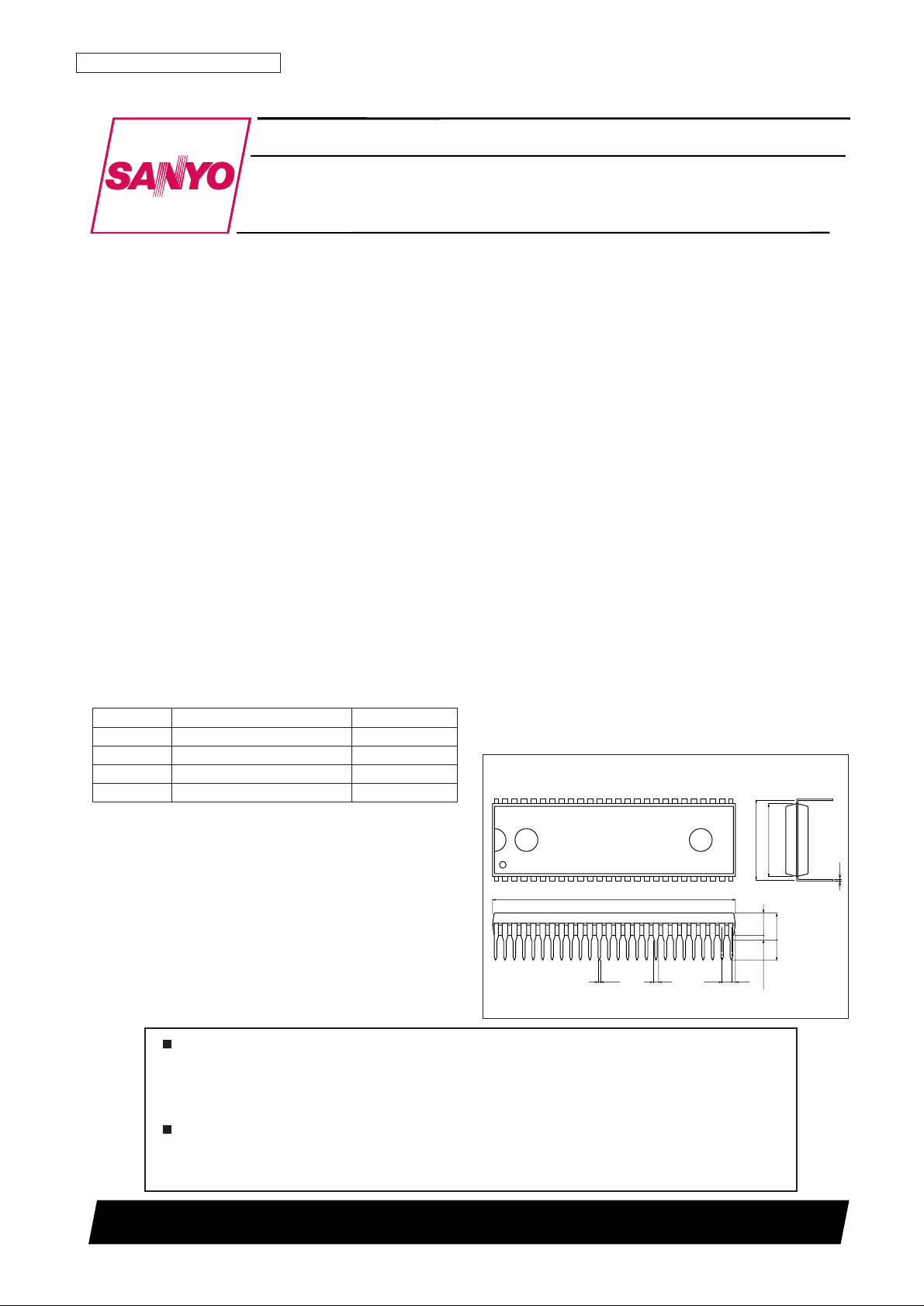
Package Dimensions
unit: mm
3128-DIP52S
46.0
0.48 1.05 1.78
0.75
4.25
15.24
0.25
13.8
0.51min
5.1max
3.8
261
2752
SANYO: DIP52S
[LA7674]
LA7674
SANYO Electric Co.,Ltd. Semiconductor Company
TOKYO OFFICE Tokyo Bldg., 1-10, 1 Chome, Ueno, Taito-ku, TOKYO, 110-8534 JAPAN
Color TV Single-Chip Signal Processor for NTSC Systems
(PLL Detection)
Monolithic Linear IC
Any and all SANYO products described or contained herein do not have specifications that can handle
applications that require extremely high levels of reliability, such as life-support systems, aircraft’s
control systems, or other applications whose failure can be reasonably expected to result in serious
physical and/or material damage. Consult with your SANYO representative nearest you before using
any SANYO products described or contained herein in such applications.
SANYO assumes no responsibility for equipment failures that result from using products at values that
exceed, even momentarily, rated values (such as maximum ratings, operating condition ranges, or other
parameters) listed in products specifications of any and all SANYO products described or contained
herein.
Delay line Video external, audio external Switch rating
OFF IN 6.9 to 9.0V
OFF EXT 4.7 to 6.6V
ON EXT 2.4 to 4.3V
ON IN 0 to 2.1V
No. 4361-2/6
LA7674
Parameter Symbol Conditions Ratings Unit
Maximum supply voltage
V11 max 11 V
V14 max 11 V
Maximum supply current I30max 16 mA
Allowable power dissipation Pd max Ta ≤ 60°C 1.35 W
Operating temperature range Topr –10 to +65 °C
Storage temperature range Tstg –55 to +150 °C
Circuit current
I44 –6 mA
I6 –3 mA
FBP input current
I22 max Peak current 5 mA
I21 max Peak current 10 mA
Specifications
Absolute Maximum Ratings at Ta = 25° C
Parameter Symbol Conditions Ratings Unit
Recommended supply voltage
V11 9V
V14 9V
Recommended supply current I30 13 mA
Operating voltage range
V11op 8 to 9.5 V
V14op 8 to 9.5 V
Operating current range I30op 10 to 16 mA
Operating Conditions at Ta = 25° C
Parameter Symbol Conditions
Ratings
Unit
min typ max
[Circuit Voltage and Current]
Horizontal supply voltage V30 V
CC
= 9V, ICC= 13mA 7.3 7.8 8.3 V
Supply current I11 + 14 V
CC
= 9V, ICC= 13mA, IFAGC 4V 102 120 138 mA
[VIF]
Quiescent video output voltage V44 Quiescent 4.3 4.7 5.1 V
Quiescent AFT output voltage V47 Quiescent 3.1 4.7 6.1 V
Maximum RFAGC voltage V49H CW = 85dBµ, RFAGCVR = min 7.6 8.0 8.3 V
Minimum RFAGC voltage V49L CW = 85dBµ, RFAGCVR = max 0 0.01 0.3 V
Input sensitivity Vi
VIF input level for video output at 0.8Vp-p
33 39 45 dBµ
(40% mod).
AGC range GR Maximum input (V0 = 0.8Vp-p) - input sensitivity 54 62 70 dB
Maximum permissible input Vi max VIF input level for video output at +1dB 97 104 111 dBµ
Video output detection V
O
44 Vi = 80dBµ, AM = 78% mod 1.7 2.0 2.3 Vp-p
Differential gain DG Vi = 80dBµ, AM = 87.5%, video mod 3.0 10 %
Differential phase DP Vi = 80dBµ, AM = 87.5%, video mod 1.0 10 DEG
Video S/N S/N Vi = 80dBµ, 20 log
1.46 (Vp-p)
47 54 61 dB
noise (Vrms)
Synchronization signal tip level V44 TIP CW = 80dBµ 2.1 2.4 2.7 V
Frequency characteristic f
C
Frequency at video output of –3dB 6.0 9.0 12.0 MHz
920 kHz VIF intermodulation I920 V3.58MHz/V920kHz, Vi = 80dBµ 35 42 49 dB
Maximum AFT output voltage V47H CW = 80dBµ, frequency change 8.3 8.7 9.0 V
Minimum AFT output voltage V47L CW = 80dBµ, frequency change 0.1 0.3 0.8 V
AFT detection sensitivity Sf CW = 80dBµ, frequency change 45 70 100 mV/kHz
AFT switch operation start voltage V
AFTSW
Measuring with sweep signal 0.5 1.0 1.5 V
Black noise threshold level V
BTH
Measuring with sweep signal 1.1 1.4 1.7 V
APC pull-in range (U)2 f
PU-2
CW = 80dBµ, fP= 53MHz to 64MHz 0.8 1.7 4.0 MHz
APC pull-in range (L)2 f
PL-2
CW = 80dBµ, fP= 53MHz to 64MHz –2 –1 MHz
VCO maximum variable range
∆f
U
Quiescent 0.9 1.7 4.0 MHz
∆f
L
Quiescent –4 –2 –1 MHz
VCO control sensitivity β Quiescent 1.5 3.0 5.5 kHz/mV
Operating Characteristics at Ta = 25°C, VCC= V11 = V14 = 9 V, ICC= I30 = 13 mA
Continued on next page.
 Loading...