

Page 1
Monolithic Linear IC
Ordering number : EN5097
61595HA (OT) No. 5097-1/11
SANYO Electric Co.,Ltd. Semiconductor Bussiness Headquarters
TOKYO OFFICE Tokyo Bldg., 1-10, 1 Chome, Ueno, Taito-ku, TOKYO, 110-8534 JAPAN
Video Signal Auto-White Processing IC
LA7668N
Overview
The LA7668N is a low-cost video signal auto-white
processing IC that provides brightness adapted
compression and expansion functions. Furthermore, the
LA7668N incorporates on-chip a Sanyo developed
vertical line saturation suppression function for image
quality enhancement.
Features and Functions
• APL; frequency adaptive Y/C correction
• Vertical line saturation suppression function
• Correction circuit on/off function
• Built-in synchronization/burst gate separation circuit
• 4.0 V band gap Zener output
• Variable correction curve (using an external resistor)
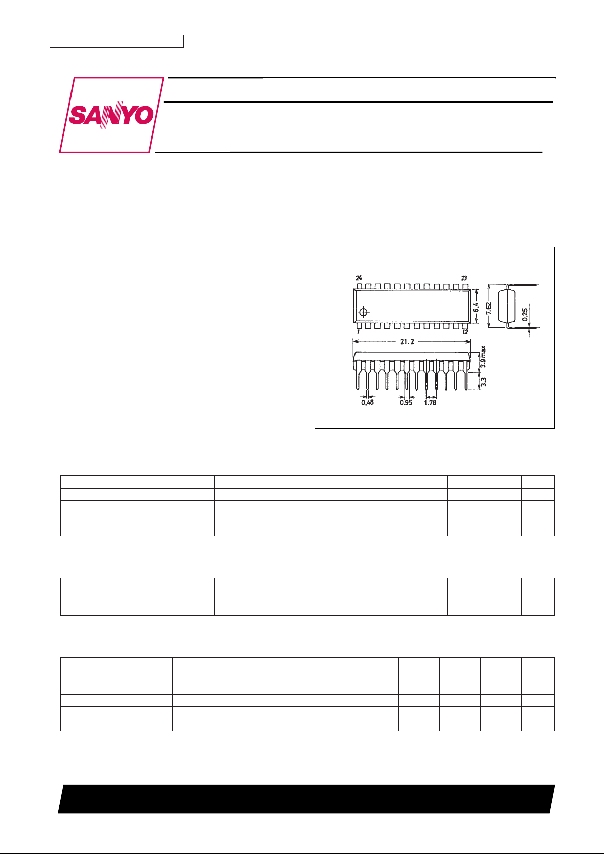
Package Dimensions
unit: mm
3067-DIP24S
Specifications
Maximum Ratings at Ta = 25°C
Operating Conditions at Ta = 25°C
Electrical Characteristics at Ta = 25°C, VCC= 5.0 V
Parameter Symbol Conditions Ratings Unit
Maximum supply voltage V
CC
max 7.0 V
Allowable power dissipation Pd max Ta ≤ 65°C 200 mW
Operating temperature Topr –10 to +65 °C
Storage temperature Tstg –55 to +125 °C
Parameter Symbol Conditions Ratings Unit
Recommended supply voltage V
CC
5.0 V
Operating supply voltage range V
CC
op 4.5 to 5.5 V
Parameter Symbol Conditions min typ max Unit
Current drain (off) I
OFF
Pin 17 = 5 V, no input 16.0 20.0 25.0 mA
Current drain (on) I
ON
Pin 17 = 0 V, no input 18.0 22.0 28.0 mA
BGZ output 1 V
BGZ1IOUT
= 3 mA 3.7 4.0 4.3 V
BGZ output 2 V
BGZ2IOUT
= 3 mA, VCC= 4.5 V 3.65 4.0 4.3 V
BGZ maximum output current I
OMAXVCC
= 4.5 V 5.0 8.0 mA
Continued on next page.
[LA7668N]
SANYO: DIP24S
Page 2
Continued from preceding page.
Pin Functions
No. 5097-2/11
LA7668N
Parameter Symbol Conditions min typ max Unit
[Luminance Signal System]
Voltage gain VG
Y
VIN= 1.0 Vp-p 6.0 6.5 7.0 dB
Frequency characteristics f
Y
When 3 dB down from the 1 MHz output level 7.0 8.5 MHz
Signal input level V
IY
1.0 1.2 Vp-p
Output DC level V
OYDC
Pedestal level 0.7 0.9 1.1 V
Pin 18 output V
18
1.75 2.0 2.25 V
γ characteristics 90 ∆
γ90
APL = 90%, VIN= 100 IRE 101 105 109 IRE
γ characteristics 50 ∆
γ50
APL = 50%, VIN= 40 IRE 41 45 49 IRE
γ characteristics 10-1 ∆
γ10-1
APL = 10%, VIN= 80 IRE 81 85 89 IRE
γ characteristics 10-2 ∆
γ10-2
APL = 10%, VIN= 40 IRE 43 47 52 IRE
[Chrominance Signal System]
Voltage gain VG
C
VIN= 0.66 Vp-p 6.3 6.8 7.2 dB
Maximum gain VG
MAX
When f = 3.58 MHz, APL = 0% 7.3 7.8 8.3 dB
Minimum gain VG
MIN
When f = 3.58 MHz, APL = 100% 5.7 6.2 6.7 dB
Frequency characteristics f
C
When 3 dB down from the 1 MHz output level 4.0 5.0 MHz
Signal input level V
IC
0.66 0.8 Vp-p
Output DC level V
OCDC
1.1 1.4 1.7 V
[Control System]
Mute on voltage V
ON
1.0 V
CC
V
Mute off voltage V
OFF
0 0.5 V
Pin 2 voltage V2 2.81 3.2 3.61 V
Pin 4 voltage V3 2.72 3.1 3.50 V
Pin 11 voltage V11 2.19 2.5 2.82 V
Pin 14 voltage V14 2.29 2.6 2.94 V
Pin 15 voltage V15 2.11 2.4 2.71 V
Pin 16 voltage V16 2.02 2.3 2.60 V
Pin 21 voltage V21 2.54 2.9 3.27 V
Pin 23 voltage V23 2.02 2.3 2.60 V
Pin No. Symbol Function
1 LPF
D
Correction signal frequency control
2 H
U
Correction reference voltage (3.2 V)
3 Y
IN
Luminance signal input
4 H
D
Correction reference voltage (3.1 V)
5 SYNC Sync separator input
6 V
CC
Power supply
7 BGP BGP delay time constant
8 APL
DET
APL level detection filter
9 HPF
IN
High-frequency detection filter (input)
10 HPF
OUT
High-frequency detection filter (output)
11 HE
DET
High-frequency detection circuit control voltage
12 C
IN
Chrominance signal input
13 C
OUT
Chrominance signal output
14 APL
H
APL discrimination reference voltage (high)
15 APL
L1
APL discrimination reference voltage (low)
16 APL
L2
APL discrimination reference voltage (for the high-frequency detection circuit)
17 MUTE Correction circuit muting
18 2.0VBIAS Luminance signal system bias
19 GND Ground
20 BGZ
OUT
4.0 V BGZ voltage output
21 L
D
Correction reference voltage (2.9 V)
22 Y
OUT
Luminance signal output
23 L
U
Correction reference voltage (2.3 V)
24 LPF
U
Correction signal frequency control
Page 3
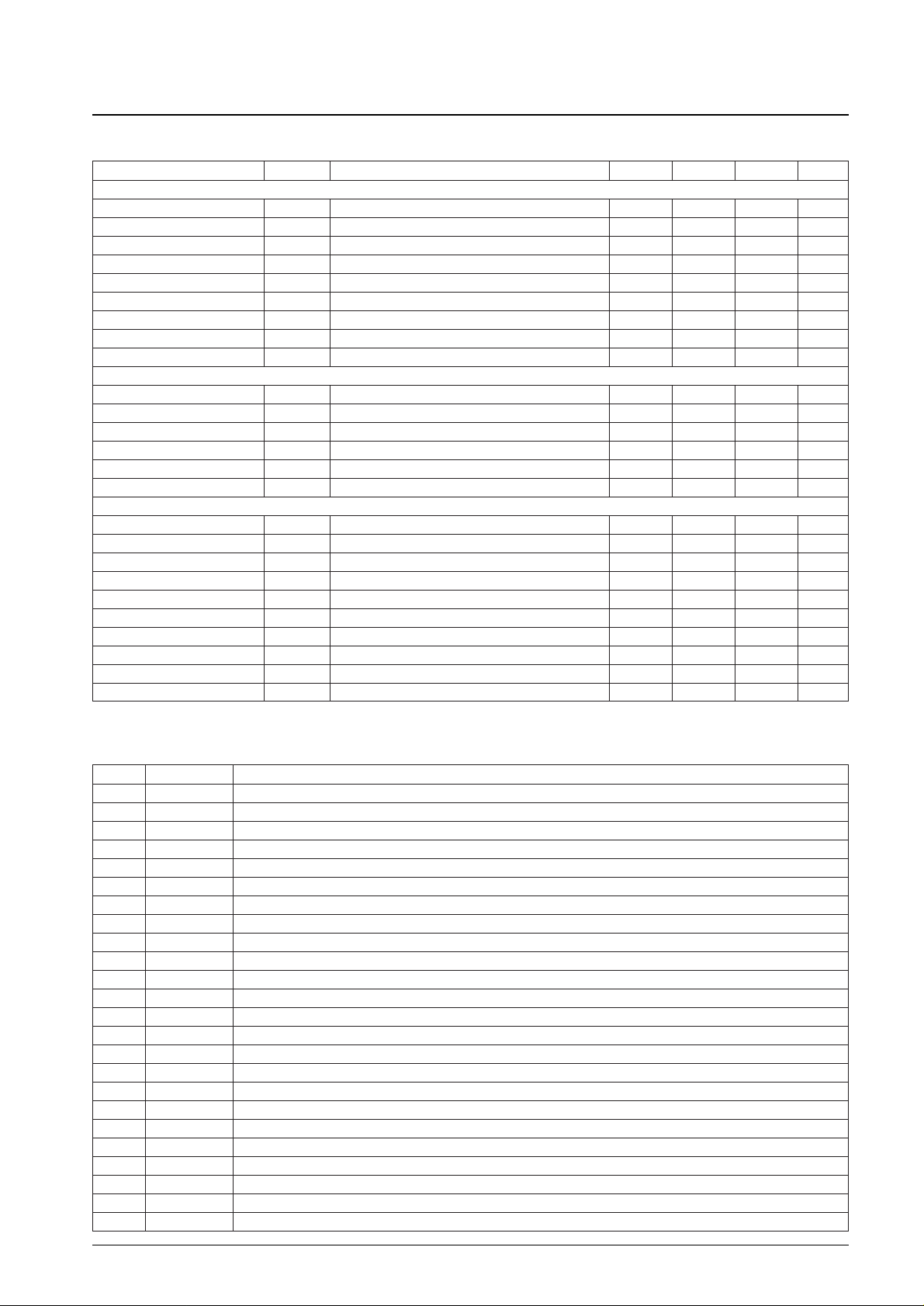
Application Circuit Diagram
No. 5097-3/11
LA7668N
Page 4
Pin Descriptions
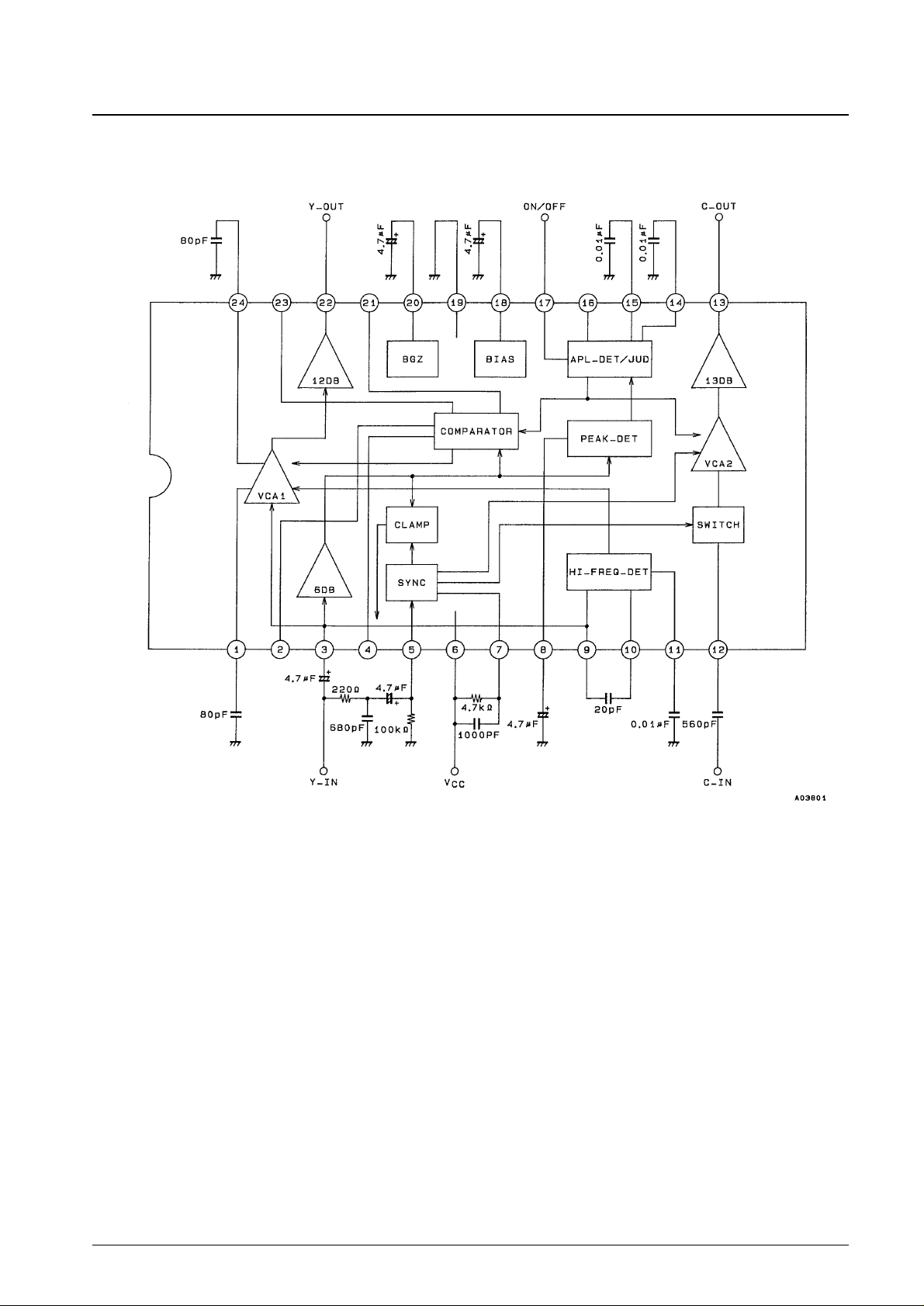
• Pins 1 and 24
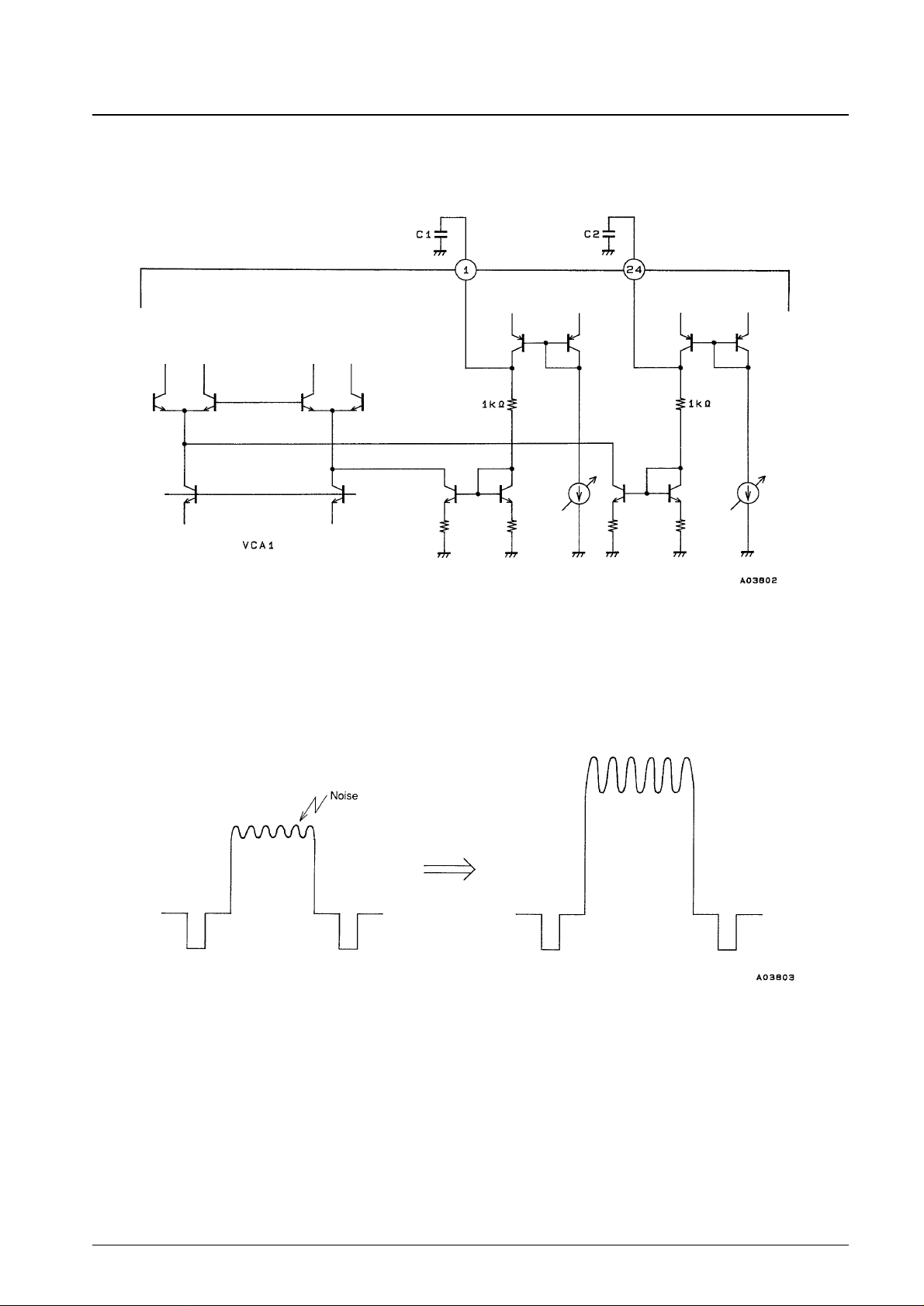
Pins 1 and 24 are frequency control pins for the correction signal. If the capacitors C1 and C2 were not connected to pins
1 and 24, when correction was applied to signals that include noise as shown in the figure below, the noise level would
increase. Accordingly, the capacitors C1 and C2 are used to reduce the high frequencies so that high-frequency noise
levels are not aggravated. (frequency-adaptive type circuit)
C1 is provided for when the gain is increased, and C2 for when the gain is decreased. About 2 MHz when C = 82 pF.
No. 5097-4/11
LA7668N
Page 5

• Pins 2, 4, 21 and 23
These are gamma correction reference voltage pins. The gamma characteristics can be changed by changing the voltages
applied to these pins from external circuits.
Pins 2 and 4 are the reference voltages used when APL is high, and pins 21 and 23 are the reference voltages used when
APL is low.
The figures below shows the characteristics curves.
No. 5097-5/11
LA7668N
Page 6

• Pin 3
Pin 3 is the luminance signal input pin.
The reference input level is 1.0 Vp-p.
• Pin 5
Pin 5 is the sync separator input pin.
• Pin 6
Pin 6 is the power supply pin. The recommended operating voltage range is 4.5 to 5.5 V. However, operation as low as
4.3 V is possible, although certain device characteristics will be degraded.
• Pin 7
Pin 7 is used to construct the filter that determines the BGP delay time.
No. 5097-6/11
LA7668N
Page 7

• Pin8
Pin 8 is used to construct the APL level detection filter.
• Pins 9 and 10
Pins 9 and 10 are used for the high-frequency detection circuit high-pass filter capacitor.
The signal input to pin 3 (the Y input signal) is accepted by an emitter-follower circuit, which outputs a signal clamped
to 2.0 V from pin 9. This 2.0 V clamped high-frequency signal is detected by the high-pass filter formed by C1. (A 2 to
3 MHz signal is detected when C1 is 20 pF.)
• Pin 11
Pin 11 is the high-frequency detection circuit control voltage pin.
The pin 11 voltage sets the high-frequency detection level. (Pin 11 should normally be set to 2.5 V.) Thus an externally
applied voltage can be used to change this detection level.
No. 5097-7/11
LA7668N
Page 8

The capacitor between pins 9 and 10 extracts the high-frequency component for vertical line saturation control. The pin
11 voltage determines the level at which saturation control is not applied. (Note that this circuit only operates when APL
is low. The operating level is determined by the pin 16 voltage.)
• Pin 12
Pin 12 is the chrominance signal input pin.
• Pin 13
Pin 13 is the chrominance signal output pin.
No. 5097-8/11
LA7668N
The chrominance signal input circuit is a
switching circuit, but could consist of a Y/C
separator. This circuit is designed to reduce the
noise due to the influence of the SYNC signal.
Page 9

• Pins 14, 15 and 16
Pins 14, 15 and 16 are the APL level reference voltage pins.
When the APL filter pin (pin 8) voltage is higher than the pin 14 reference voltage (2.6 V), the APL level is judged to be
high. If that voltage is lower than the pin 15 reference voltage, the APL level is judged to be low. Pin 16 is a reference
voltage for the high-frequency detection circuit, and the vertical line saturation suppression circuit operates when the pin
8 voltage is lower than the pin 16 voltage. See the description of the APL filter voltage characteristics on page 10 for
details on the relationship between the APL level and the APL filter pin voltage.
• Pin 17
Pin 17 mutes the correction circuit.
• Pin 18
Pin 18 is the 2.0 V Y signal system reference voltage pin.
This reference voltage pin determines the Y signal system clamp and output voltages. C1 is used to exclude noise from
the reference voltage line.
No. 5097-9/11
LA7668N
Page 10

• Pin 19
Pin 19 is the IC ground pin.
• Pin 20
Pin 20 is the BGZ output voltage pin. C1 is used to exclude noise and prevent oscillation. The pin 20 circuit can supply
an output current of up to 4 mA when VCCis 4.5 V. Note that if VCCis under 4.3 V, the pin 20 voltage will become
lower due to the influence of the transistor’s VCE. (The IC can be operated with VCCas low as 4.3 V if an output
current is not taken from this pin.) The figure below shows the output voltage vs. current characteristics, i.e., the BGZ
output voltage characteristics.
• Pin 22
Pin 22 is the Y output pin.
No. 5097-10/11
LA7668N
Page 11

PS No. 5097-11/11
LA7668N
Characteristic Output Waveforms
This catalog provides information as of June, 1995. Specifications and information herein are subject to change
without notice.
■ No products described or contained herein are intended for use in surgical implants, life-support systems, aerospace
equipment, nuclear power control systems, vehicles, disaster/crime-prevention equipment and the like, the failure of
which may directly or indirectly cause injury, death or property loss.
■ Anyone purchasing any products described or contained herein for an above-mentioned use shall:
➀ Accept full responsibility and indemnify and defend SANYO ELECTRIC CO., LTD., its affiliates, subsidiaries and
distributors and all their officers and employees, jointly and severally, against any and all claims and litigation and all
damages, cost and expenses associated with such use:
➁ Not impose any responsibility for any fault or negligence which may be cited in any such claim or litigation on
SANYO ELECTRIC CO., LTD., its affiliates, subsidiaries and distributors or any of their officers and employees
jointly or severally.
■ Information (including circuit diagrams and circuit parameters) herein is for example only; it is not guaranteed for
volume production. SANYO believes information herein is accurate and reliable, but no guarantees are made or implied
regarding its use or any infringements of intellectual property rights or other rights of third parties.
 Loading...