

Overview
The LA76070 is an NTSC color television IC. In addition
to providing IIC bus control based rationalization of IC
control and the adjustment manufacturing process
associated with the TV tube itself, it also includes all
functions actually required in mass-produced television
sets. As such, it is an extremely practical bus control IC.
* The LA7840/41 or LA7845N/46N is recommended as the vertical output
IC for use with this product.
Functions
•I2C bus control, VIF, SIF, Y, C, and deflection
integrated on a single chip.
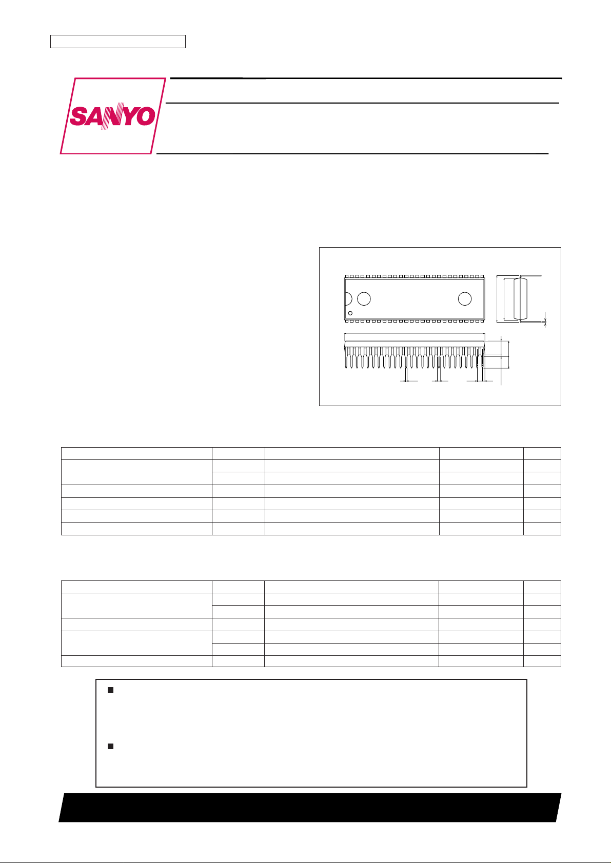
Package Dimensions
unit: mm
3128-DIP52S
46.0
0.48 1.05 1.78
0.75
4.25
15.24
0.25
13.8
0.51min
5.1max
3.8
261
2752
Monolithic Linear IC
Ordering number : ENN5844
70999 RM (OT) No. 5844-1/27
SANYO: DIP52S
[LA76070]
SANYO Electric Co.,Ltd. Semiconductor Company
TOKYO OFFICE Tokyo Bldg., 1-10, 1 Chome, Ueno, Taito-ku, TOKYO, 110-8534 JAPAN
NTSC Color Television IC
LA76070
Specifications
Maximum Ratings at Ta = 25°C
Note: *Provided on a printed circuit board: 83.2 × 86.0 × 1.6 mm, material: Bakelite
Operating Conditions at Ta = 25°C
Parameter Symbol Conditions Rating Unit
Maximum power supply voltage
V4 max 9.6 V
V26 max 9.6 V
Maximum power supply current I21 max 25 mA
Allowable power dissipation Pd max Ta ≤ 65°C* 1.3 W
Operating temperature Topr –10 to +65 °C
Storage temperature Tstg –55 to +150 °C
Parameter Symbol Conditions Rating Units
Recommended power supply voltage
V4 7.6 V
V26 7.6 V
Recommended power supply current I21 19 mA
Operating power supply voltage range
V4 op 7.3 to 7.9 V
V26 op 7.3 to 7.9 V
Operating power supply current range 121 op 16 to 25 mA
Any and all SANYO products described or contained herein do not have specifications that can handle
applications that require extremely high levels of reliability, such as life-support systems, aircraft’s
control systems, or other applications whose failure can be reasonably expected to result in serious
physical and/or material damage. Consult with your SANYO representative nearest you before using
any SANYO products described or contained herein in such applications.
SANYO assumes no responsibility for equipment failures that result from using products at values that
exceed, even momentarily, rated values (such as maximum ratings, operating condition ranges, or other
parameters) listed in products specifications of any and all SANYO products described or contained
herein.
Electrical Characteristics at Ta = 25°C, VCC= V4 = V26 = 7.6 V, ICC= I21 = 19 mA
No. 5844-2/27
LA76070
Continued on next page.
Parameter Symbol Conditions
Ratings
Unit
min typ max
[Circuit Voltages and Currents]
Horizontal power supply voltage HV
CC
7.2 7.6 8.0 V
IF power supply current (V4) I4 (IFI
CC
) IF AGC: 5 V 38 46 54 mA
Video, chroma,
I26 (YCVI
CC
) 79.5 93.5 107.5 mA
and vertical power supply current (V26)
[VIF Block]
AFT output voltage with no signal VAFTn With no input signal 2.8 3.8 4.8 Vdc
Video output voltage with no signal VOn With no input signal 4.7 4.9 5.1 Vdc
APC pull-in range (U) fPU After APC and PLL DAC adjustment 1.0 MHz
APC pull-in range (L) fPL After APC and PLL DAC adjustment 1.0 MHz
Maximum RF AGC voltage VRFH CW = 91 dBµ, DAC = 0 7.7 8.2 9.0 Vdc
Minimum RF AGC voltage VRFL CW = 91 dBµ, DAC = 63 0 0.2 0.4 Vdc
RF AGC Delay Pt (@DAC = 0) RFAGC0 DAC = 0 96 dBµ
RF AGC Delay Pt (@DAC = 63) RFAGC63 DAC = 63 86 dBµ
Maximum AFT output voltage VAFTH CW = 93 dBµ, variable frequency 6.2 6.5 7.6 Vdc
Minimum AFT output voltage VAFTL CW = 93 dBµ, variable frequency 0.5 0.9 1.2 Vdc
AFT detection sensitivity VAFTS CW = 93 dBµ, variable frequency 33 25 17 mV/kHz
Video output amplitude VO 93 dBµ, 87.5% Video MOD 1.8 2.0 2.2 Vp-p
Synchronization signal tip level VOtip 93 dBµ, 87.5% Video MOD 2.4 2.6 2.8 Vdc
Input sensitivity Vi Output at –3 dB 43 46 dBµ
Video-to-sync ratio (@100 dBµ) V/S 100 dBµ, 87.5% Video MOD 2.4 2.5 3.0
Differential gain DG 93 dBµ, 87.5% Video MOD 2 10 %
Differential phase DP 93 dBµ, 87.5% Video MOD 2 10 deg
Video signal-to-noise ratio S/N CW = 93 dBµ 55 58 dB
920 kHz beat level I920 V3.58 MHz/V920 kHz –50 dB
[Video and Switching Block]
External video gain AUXG Stair step, 1 V p-p 5.5 6.0 6.5 dB
External video sync signal tip voltage AUXS Stair step, 1 V p-p –0.2 0.0 +0.2 Vdc
External video crosstalk AUXC 4.2 MHz, 1Vp-p 60 dB
Internal video output level INTO 93 dBµ, 87.5% Video MOD –0.1 0.0 +0.1 Vp-p
[SIF Block]
FM detector output voltage SOADJ 464 474 484 mVrms
FM limiting sensitivity SLS Output at –3 dB 50 dBµ
FM detector output bandwidth SF Output at –3 dB 50 100 k Hz
FM detector output total
STHD FM = ±25 kHz 0.5 %
harmonic distortion
AM rejection ratio SAMR AM = 30 % 40 dB
SIF signal-to-noise ratio SSN 60 dB
[Audio Block]
Maximum gain AGMAX 1 kHz –2.5 0.0 +2.5 dB
Adjustment range ARANGE 60 67 dB
Frequency characteristics AF 20 kHz –3.0 +3.0 dB
Muting AMUTE 20 kHz 75 dB
Total harmonic distortion ATHD 1 kHz, 400 m Vrms, Vo1: MAX 0.5 dB
Signal-to-noise ratio ASN DIN.Audio 65 75 dB
[Chroma Block]
ACC amplitude characteristics 1 ACCM1 Input: +6 dB/0 dB, 0 dB = 40 IRE 0.8 1.0 1.2 times
ACC amplitude characteristics 2 ACCM2 Input: –14 dB/0 dB 0.7 1.0 1.1 times
B-Y/Y amplitude ratio CLRBY 100 125 140 %
Color control characteristics 1 CLRMN Color MAX/NOM 1.6 1.8 2.1 times
Color control characteristics 2 CLRMM Color MAX/MIN 33 40 50 dB
Continued on next page.
Continued from preceding page.
No. 5844-3/27
LA76070
Parameter Symbol Conditions
Ratings
Unit
min typ max
Color control sensitivity CLRSE 1 2 4 %/bit
Tint center TINCEN TINT NOM –15 –3 deg
Tint control maximum TINMAX TINT MAX 30 45 60 deg
Tint control minimum TINMIN TINT MIN –60 –45 –30 deg
Tint control sensitivity TINSE 0.7 2.0 deg/bit
Demodulator output ratio R-Y/B-Y RB 0.75 0.85 0.95
Demodulator output ratio G-Y/B-Y GB 0.28 0.33 0.38
Demodulator angle B-Y/R-Y ANGBR 92 99 107 deg
Demodulator angle G-Y/B-Y ANGGB 227 237 247 deg
Killer operating point KILL 0 dB = 40 IRE –42 –37 –30 dB
Chrominance VCO free-running frequency
CVCOF Deviation from 3.579545 MHz –350 +350 Hz
Chrominance pull-in range (+) PULIN+ 350 Hz
Chrominance pull-in range (–) PULIN– –350 Hz
Auto-flesh characteristic 73° AF 073 5 10 20 deg
Auto-flesh characteristic 118° AF 118 –7 0 +7 deg
Auto-flesh characteristic 163° AF 163 –20 –10 –5 deg
[Video Block]
Overall video gain
CONT63 10 12 14 dB
(Contrast set to maximum)
Contrast adjustment characteristic
CONT32 –7.5 –6.0 –4.5 dB
(Normal/maximum)
Contrast adjustment characteristic
CONT0 –17 –14 –11 dB
(Minimum/maximum)
Video frequency characteristic
Yf0 –6.0 –3.5 0.0 dB
Trap & D = 0
Chrominance trap level
Ctrap –20 dB
Trap & D = 1
DC propagation ClampG 95 100 105 %
Y delay, f0 = 1 YDLY 430 ns
Maximum black stretching gain BKSTmax 6 13 20 IRE
(normal) Sharp16 4 6 8 dB
Sharpness adjustment range (max) Sharp31 9.0 11.5 14.0 dB
(min) Sharp0 –6.0 –3.5 –1.0 dB
Horizontal/vertical blanking output level RGBBLK 1.4 1.6 1.8 V
[OSD Block]
OSD fast switch threshold FSTH 0.9 1.2 1.7 V
Red RGB output level ROSDH 220 250 280 IRE
Green RGB output level GOSDH 220 250 280 IRE
Blue RGB output level BOSDH 220 250 280 IRE
Analog OSD R output level
RRGB 1.5 1.9 2.3 Ratio
gain matching
Linearity LRRGB 45 50 60 %
Analog OSD G output level
GRGB 1.5 1.9 2.3 Ratio
gain matching
Linearity LGRGB 45 50 60 %
Analog OSD B output level
BRGB 1.5 1.9 2.3 Ratio
gain matching
Linearity LBRGB 45 50 60 %
[RGB Output (cutoff and drive) Block]
Brightness control (normal) BRT64 2.1 2.65 3.2 V
High brightness (maximum) BRT127 15 20 25 IRE
Low brightness (minimum) BRT0 –25 –20 –15 IRE
Continued on next page.
Continued from preceding page.
No. 5844-4/27
LA76070
Parameter Symbol Conditions
Ratings
Unit
min typ max
Cutoff control
(minimum) Vbias0 2.1 2.65 3.2 V
(Bias control)
(maximum) Vbias127 2.45 3.0 3.55 V
Resolution Vbiassns 4 mV/Bit
Maximum output
RBout127 2.9 Vp-p
Drive adjustment Gout127 2.4 Vp-p
Output attenuation RBout0 7 9 11 dB
[Deflection Block]
Sync separator sensitivity Ssync 3 8 13 IRE
Horizontal free-running frequency
∆fH 15600 15734 15850 Hz
deviation
Horizontal pull-in range fH PULL ±400 Hz
Horizontal output pulse saturation
V Hsat 0 0.06 0.4 V
voltage
Horizontal output pulse phase HPHCEN 9.5 10.5 11.5 µs
Horizontal position adjustment range HPHrange 4 bits ±2 µs
Horizontal position adjustment
HPHstep 530 ns
maximum variability
X-ray protection circuit operating
VXRAY 0.54 0.64 0.74 V
voltage
[Vertical screen Size Adjustment]
Vertical ramp output amplitude @32 Vsize32 VSIZE: 100000 0.47 0.82 1.17 Vp-p
Vertical ramp output amplitude @0 Vsize0 VSIZE: 000000 0.13 0.48 0.83 Vp-p
Vertical ramp output amplitude @63 Vsize63 VSIZE: 111111 0.80 1.15 1.50 Vp-p
[Vertical screen Position Adjustment]
Vertical ramp DC voltage @32 Vdc32 VDC: 100000 3.6 3.8 4.0 Vdc
Vertical ramp DC voltage @0 Vdc0 VDC: 000000 3.2 3.4 3.6 Vdc
Vertical ramp DC voltage @63 Vdc63 VDC: 111111 4.0 4.2 4.4 Vdc

LA76070 BUS: Initial Conditions
No. 5844-5/27
LA76070
Initial test conditions
Register
T Enable 0 HEX
Video Mute 1 HEX
Sync Kill 0 HEX
AFC Gain 0 HEX
Horizontal Phase 4 HEX
IF AGC SW 0 HEX
AFT Defeat 0 HEX
RF AGC Delay 20 HEX
Initial test conditions (continued)
Register
Video SW 0 HEX
PLL Tuning 40 HEX
Audio Mute 1 HEX
APC Det Adjust 20 HEX
V CD Mode 0 HEX
Vertical DC 20 HEX
Vertical Kill 0 HEX
Col Kill 0 HEX
Vertical Size 20 HEX
Red Bias 00 HEX
Green Bias 00 HEX
Blue Bias 00 HEX
Blanking Defeat 0 HEX
Red Drive 7F HEX
Blue Drive 7F HEX
Color Difference Mode Enable 0 HEX
Brightness Control 40 HEX
Contrast Test Enable 0 HEX
Contrast Control 40 HEX
Trap & Delay Enable SW 0 HEX
Auto Flesh 0 HEX
Black Stretch Defeat 0 HEX
Sharpness Control 10 HEX
Tint Test Enable 0 HEX
Tint Control 40 HEX
Color Test Enable 0 HEX
Color Control 40 HEX
Vertical Test 0 HEX
Video Level 4 HEX
FM Level 10 HEX
BNI Enable 0 HEX
Audio SW 0 HEX
Volume Control 00 HEX

No. 5844-6/27
LA76070
LA76070 BUS: Control Register Descriptions
Control register descriptions
Register name Bits General descriptions
T Enable 1 Disable the Test SW & enable Video Mute SW
Video Mute 1 Disable video outputs
Sync Kill 1 Force free-run mode
AFC Gain 1 Select horizontal first loop gain
Horizontal Phase 3 Align sync to flyback phase
IF AGC SW 1 Disable IF and RF AGC
AFT Defeat 1 Disable AFT output
RF AGC Delay 6 Align RF AGC threshold
Video SW 1 Select Video Signal (INT/EXT)
PLL Tuning 7 Align IF VCO frequency
Audio Mute 1 Disable audio outputs
APC Det Adjust 6 Align AFT crossover
V Count Down Mode 1 Select vertical countdown mode
Vertical DC 6 Align vertical DC bias
Vertical Kill 1 Disable vertical output
Color Kill 1 Enable Color Killer
Vertical Size 6 Align vertical amplitude
Red Bias 7 Align Red OUT DC level
Green Bias 7 Align Green OUT DC level
Blue Bias 7 Align Blue OUT DC level
Blanking Defeat 1 Disable RGB output blanking
Red Drive 6 Align Red OUT AC level
Drive Test 1 Enable drive DAC test mode
Blue Drive 6 Align Blue OUT AC level
Color Difference Mode Enable 1 Enable color difference mode
Brightness Control 7 Customer brightness control
Contrast Test 1 Enable Contrast DAC test mode
Contrast Control 7 Customer Contrast control
Trap & Delay-SW 1 Select luma filter mode
Auto Flesh Enable 1 Enable autoflesh function
Black Stretch Defeat 1 Disable black stretch
Sharpness Control 5 Customer sharpness control
Tint Test 1 Enable tint DAC test mode
Tint Control 7 Customer tint control
Color Test 1 Enable color DAC test mode
Color Control 7 Customer color control
Vertical Test 3 Select vertical DAC test modes
Video Level 3 Align IF video level
FM Level 5 Align WBA output level
BNI Enable 1 Enable black noise inverter
Audio SW 1 Select Audio Signal (INT/EXT)
Volume Control 6 Customer volume control

No. 5844-7/27
LA76070
LA76070 BUS: Control Register Truth Table
Control register truth table
Register name 0 HEX 1 HEX
T Enable Test Enable Test Disable
Audio Mute Active Mute
Video Mute Active Mute
Sync Kill Sync active Sync Killed
AFC Gain Slow Fast
IF AGC SW AGC active AGC Defeat
AFT Defeat AFT active AFT Defeat
BNI Enable BNI active BNI Defeat
Count Down Mode Standard Non-Stand
Vertical Kill Vrt active Vrt Killed
F0 Select 3.58 trap 8.00 APF
Auto Flesh Enable AF Off AF On
Overload Enable Ovld Off Ovld On
Tint DAC Test Normal Test Mode
Color DAC Test Normal Test Mode
Contrast DAC Test Normal Test Mode
Drive DAC Test Normal Test Mode
Black Stretch Defeat Blk Str On Blk Str Off
Blanking Defeat Blanking No Blank
Color Diff Mode Enable RGB Mode C Diff Mode
Vertical Test Normal Ver Size Test
No. 5844-8/27
LA76070
LA76070 Bit Map (‘96.08.01)
IC address: BAH (101111010)
Sub address MSB DATA LSB
D0....D7 DA0 DA1 DA2 DA3 DA4 DA5 DA6 DA7
$00 * * * * T_Enable * Vid_Mute Sync_Kill
(tr0) 0 1 0
$01 * * * * AFC Gain H_Phase
(tr1) 0 1 0 0
$02 IFAGC SW AFT DEF RF_AGC_Delay
(tr2) 0 0 1 0 0 0 0 0
$03 VIDEO SW PLL TUNING
(tr3) 0 1 0 0 0 0 0 0
$04 * Aud_Mute APC DET ADJUST
(tr4) 1 1 0 0 0 0 0
$05 V CD MODE * Ver_dc
(tr5) 0 1 0 0 0 0 0
$06 Ver_kill Col_kill Ver_Size
(tr6) 0 0 1 0 0 0 0 0
$07 * R_Bias
(tr7) 0 0 0 0 0 0 0
$08 * G_Bias
(tr8) 0 0 0 0 0 0 0
$09 * B_Bias
(tr9) 0 0 0 0 0 0 0
$0A BLK_DEF R_Drive
(tr10) 0 1 1 1 1 1 1 1
$0B Drv_Test B_Drive
(tr11) 0 1 1 1 1 1 1 1
$0C C_Diff Bright
(tr12) 0 1 0 0 0 0 0 0
$0D Cot_Test Contrast
(tr13) 0 1 0 0 0 0 0 0
$0E Trap & D_SW A Fresh Black ST Sharpness
(tr14) 0 0 0 1 0 0 0 0
$0F Tint_Test Tint
(tr15) 0 1 0 0 0 0 0 0
$10 Col_Test Color
(tr16) 0 1 0 0 0 0 0 0
$11 * * * * * V_test
(tr17) 0 0 0
$12 VIDEO LEVEL FM LEVEL
(tr18) 1 0 0 1 0 0 0 0
$13 N/I SW AUDIO SW VOLUME
(tr19) 0 0 0 0 0 0 0 0

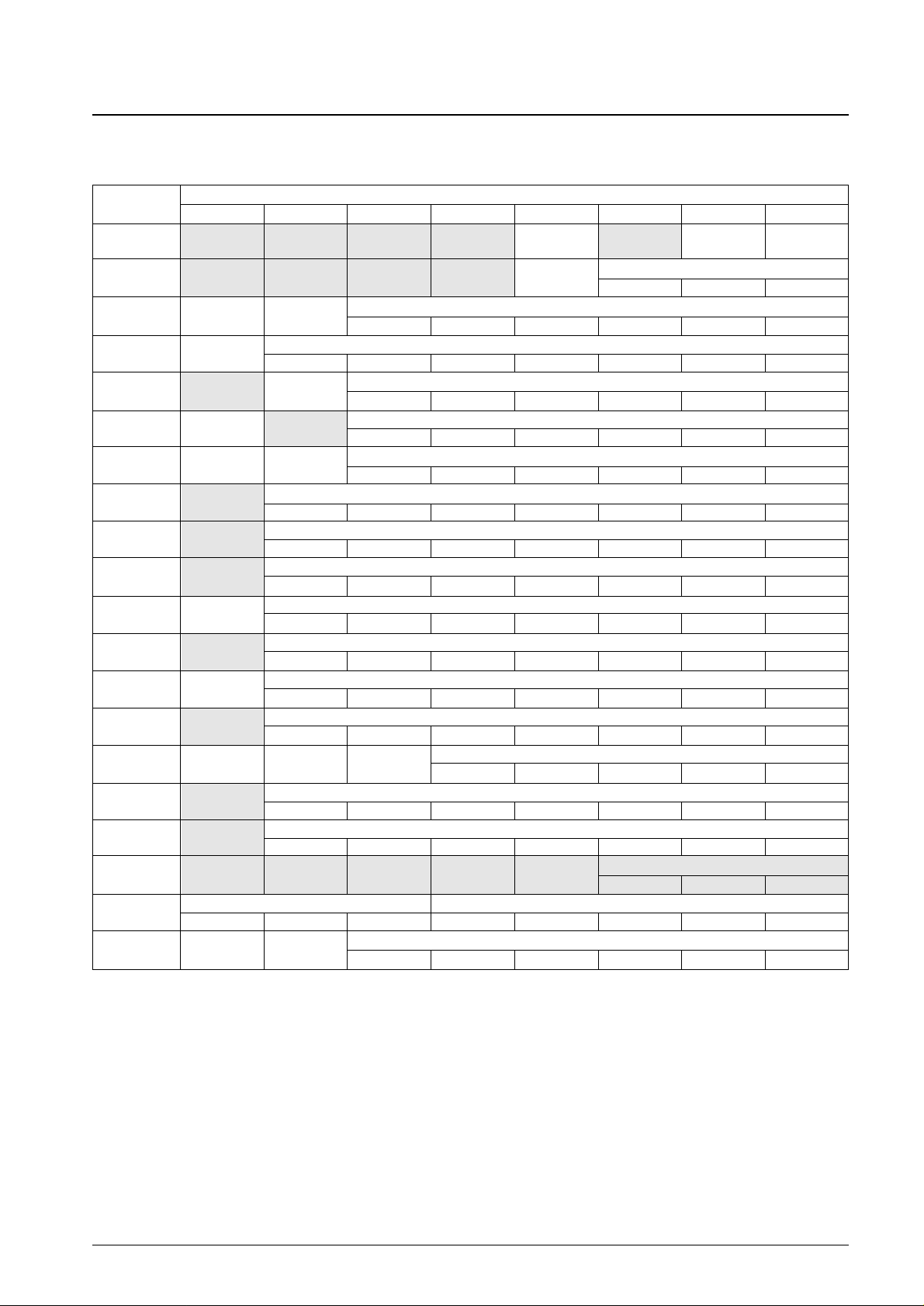
Measurement Conditions at Ta = 25°C, VCC= V4 = V26 = 7.6 V, ICC= I21= 19 mA
No. 5844-9/27
LA76070
Parameter Symbol
Measurement
Input signal Measurement method Bus conditions
point
[Circuit Voltages and Currents]
Horizontal power supply voltage HV
CC
Apply a 19mA current to pin 21 and
Initial conditions
measure the pin 21 voltage at that time
I4
Apply a voltage of 7.6 V to pin 4 and
IF power supply current (pin 4)
(IFI
CC
)
No signal measure (in mA) the DC current that flows into the IC. Initial conditions
(Apply 5 V to the IF AGC.)
Video/vertical power supply current I26 Apply a voltage of 7.6 V to pin 26 and
Initial conditions
(pin 26) (DEFI
CC
) measure (in mA) the DC current that flows into the IC
21
26
4
 Loading...