

SANYO LA7583 Datasheet
Ordering number: EN5177
Monolithic Linear IC
LA7583
(A
Overview
The LA7583 is a VIF + SIF IC that requires no adjustments. In
order to eliminate the need for adjustments in the VIF block, a
multi-network PLL has been developed and adopted for video
detection. In the SIF block, adjustments were eliminated by
using gyrator technology in the FM quadrature detector. In
addition to eliminating the need for adjustments, a buzz
canceller that suppresses Nyquist buzz has been built into the
LA7583 in order to provide excellent sound quality.
Features
.
Elimination of VCO, AFT, and SIF coils eliminates the need
for adjustments.
.
A variety of built-in filters.
.
Built-in buzz canceller results in excellent audio
characteristics.
2
Note: A
C Automatic Adjustment Control
AQT Automatic Quadrature Tuning
2
C PLL VIF + SIF) for TVs and VCRs
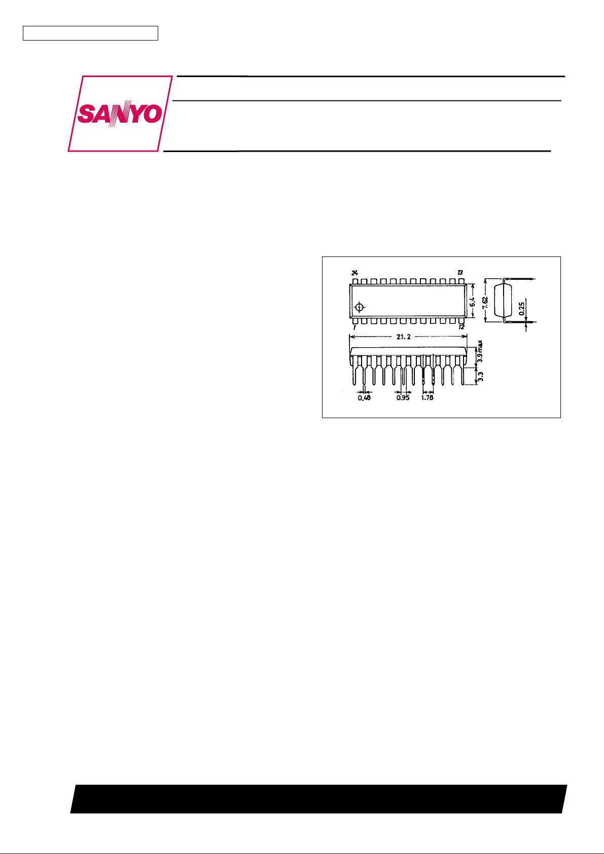
Package Dimensions
unit : mm
3067-DIP24S
[LA7583]
SANYO : DIP24S
IF Signal Processing Circuit
Functions
[VIF]
.
VIF amplifier
.
Equalizer amplifier
.
AGC lag lead filter
[1st SIF]
.
Preamplifier
[SIF]
.
Limiter amplifier
[mute]
.
Audio mute
.
Multinetwork PLL
.
AFT
.
Video driver
.
1st SIF detector
.
AQT detector (gyrator)
.
AV mute
.
BNC
.
IFAGC
.
AGC detector
.
J/U switch
.
FAGC
.
Buzz canceller
.
Built-in AGC filter
SANYO Electric Co.,Ltd. Semiconductor Bussiness Headquarters
TOKYO OFFICE Tokyo Bldg., 1-10, 1 Chome, Ueno, Taito-ku, TOKYO, 110 JAPAN
83095HA(II) No.5177-1/15
LA7583
Specifications
Maximum Ratings atTa=25°C
Parameter Symbol Conditions Ratings Unit
V
17V
Maximum supply voltage
Circuit voltage
Circuit current I1, I10, I23 –1 mA
Allowable power dissipation Pd max T
Operating temperature Topr –20 to +70
Storage temperature Tstg –55 to +150
*A2C (Automatic Adjustment Control)
Note: Current flowing into the IC is positive (no signal) and current flowing out is negative.
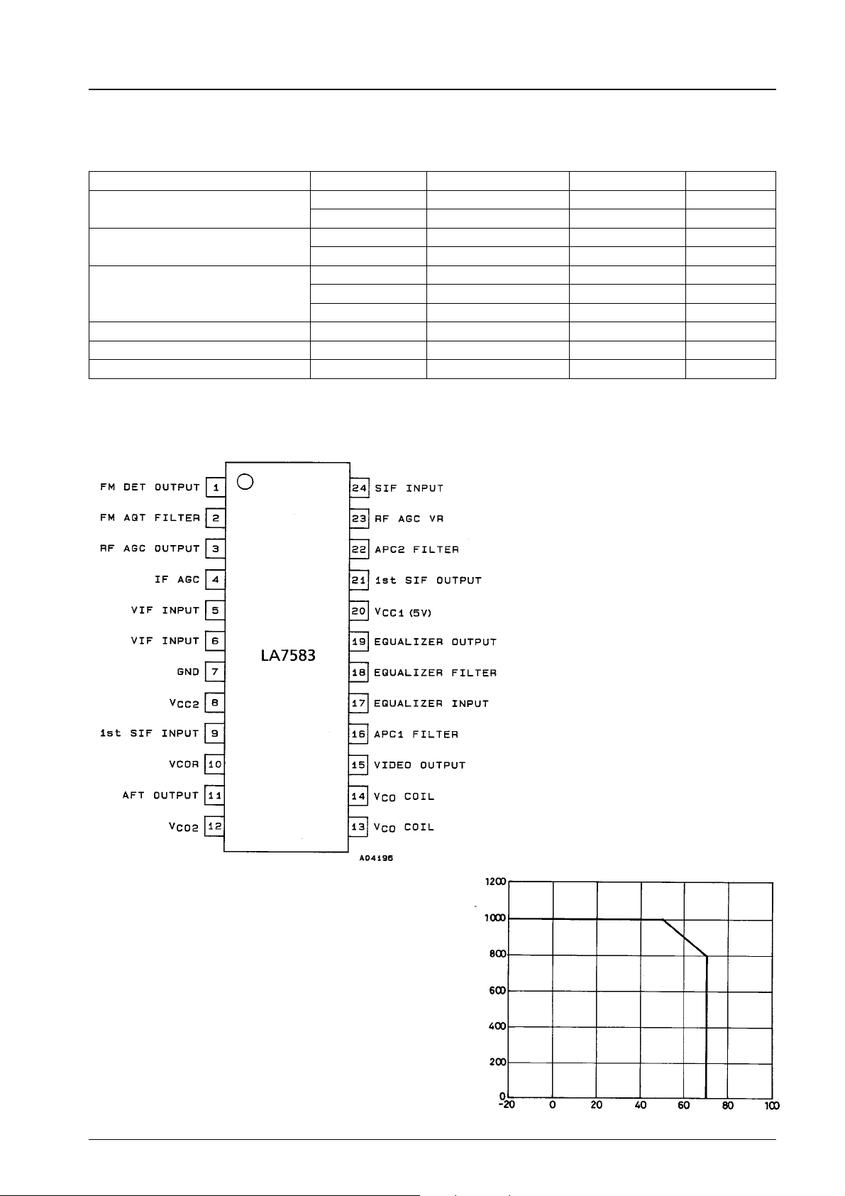
Pin Assignment
CC
V
2 13.2 V
CC
V4 V
V3, V11 V
I3, I21 –3 mA
I15, I19 –5 mA
% 50°C 1000 mW
a
1V
CC
2V
CC
C
°
C
°
Top View
Pd max — Ta
Allowable power dissipation, Pd max − mW
Ambient temperature, Ta −°C
No.5177-2/15
LA7583
Operating Conditions atTa=25°C
Parameter Symbol Conditions Ratings Unit
V
15V
Recommended supply voltage
Operating supply voltage range
Electrical Characteristics atTa=25°C, VCC1=5V,VCC2 = 9 V, fp = 45.75 MHz
Parameter Symbol Conditions min typ max Unit
[VIF Block]
Circuit current 1 I20 V
Circuit current 2 I8 V
Maxinum RF AGC voltage V3H V4=3V 7.5 8.1 9 V
Mininum RF AGC voltage V3L V4 = 1.5 V 0 +0.5 V
Input sensitivity Vi S1 = OFF 32 38 44 dBµ
AGC range G
Maxinum Allowable Input Vi max 95 103 dBµ
Video output voltage
with no signal
Sync signal tip voltage V19(tip) Vi = 10 mV 1.1 1.4 1.7 V
Video output amplitude V
Black noise threshold level
voltage
Black noise clamp voltage V
Output S/N S/N 48 52 dB
920 kHz beat level I920 P = 0, C = –10 dB, S = –10 dB 41 45 dB
Frequency characteristics f
Differential gain DG Vi = 10 mV, 87.5% 3 8 %
Differential phase DP 10STAR STEP 3 8 rad
AFT output voltage
with no signal
Maxinum AFT output voltage V11H 7.5 8.5 9 V
Mininum AFT output voltage V11L 0 +1 +1.5 V
AFT detection sensitivity Sf 33 48 69
VIF input resistance Ri(VIF) f = 45.75 MHz 0.8 1.1 1.5 kΩ
VIF input capacity Ci(VIF) f = 45.75 MHz 2 3 5 pF
APC pull-in range (U) f
APC pull-in range (L) f
AFT crossover frequency ∆f
VCO1 maximum variable range
VCO2 maximum variable range
VCO1 control sensitivity β1 V22 = 2.8 V to 3.2 V 2.4 4.8 9.6
VCO2 control sensitivity β2 V16 = 2.8 V to 3.2 V 0.3 0.6 1.2
[1st SIF Block]
4.5 MHz output gain VG Vi=1mV,41.25 MHz 23 26 29 dB
4.5 MHz output level SO Vi = 10 mV, 41.25 MHz 50 85 120 mVrms
1st SIF maximum input level Si (max) So + 12 dB–1dB 60 70 mVrms
1st SIF input resistance Ri (SIF1) f = 41.25 MHz 1.2 2 kΩ
1st SIF input capacity Ci (SIF1) f = 41.25 MHz 3 6 pF
R
V19 V4=2V 3.3 3.6 3.9 V
(V) 87.5% mod 1.7 2.0 2.3 Vp-p
O
V
BTH
BCL
C
V11 0.3 4.5 8.7 V
PU
PL
A
∆f
1 V22=4V 2.0 5.0 MHz
U
∆f
1 V22=2V –5.0 –2.0 MHz
L
∆f
2 V16=4V 100 200 kHz
U
∆f
2 V16=2V –1000 –200 kHz
L
CC
V
29V
CC
V
1 4.6 to 6 V
CC
V
2 7 to 12 V
CC
= 5 V 57 66 78 mA
CC
= 9 V 7.8 11.0 14.0 mA
CC
56 62 dB
0.4 0.7 1.1 V
1.65 1.95 2.25 V
P = 0, S = –14 dB 6 8 MHz
mV/kHz
1.0 3 MHz
–4.5 –1.0 MHz
–65 +65 kHz
kHz/mV
kHz/mV
Continued next page.
No.5177-3/15

LA7583
Continued from preceding page.
Parameter Symbol Conditions min typ max Unit
[SIF Block]
SIF limiting sensitivity Vi (lim) ∆f = 25 kHz, 400 Hz 47 53 59 dBµ
FM detection output voltage V
AMR AMR AM = 30%, 400 Hz 40 56 dB
Total harmonic distortion THD ∆f = 25 kHz, 400 Hz 0.4 1.5 %
SIF S/N S/N(SIF) ∆f = 25 kHz, 400 Hz 55 59 dB
[Mute defeat]
FM mute V24T 0.5 1.0 V
AFT defeat voltage VD11 3.9 4.5 5.1 V
J/U SW start voltage VJU24 1.5 2.0 2.5 V
AV mute voltage VM23 1 1.5 V
Vi = 100 mV, ∆f = 25 kHz, 400 Hz 300 400 520 mVrms
O
No.5177-4/15
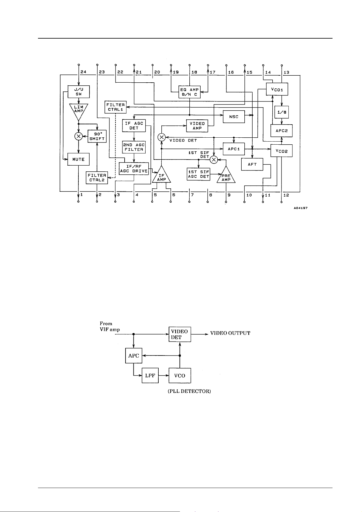
Equivalent Circuit Block Diagram
LA7583
Multinetwork PLL (Automatic Adjustment Control)
The LA7583’s PIF detector uses a multinetwork PLL and a buzz canceller. The multinetwork PLL is a PLL detector that was
developed in order to eliminate the need for adjustments in video detection.
This PLL detector offers the following features:
(1) Eliminates the need for adjustments in video detection.
(2) The PLL detection characteristics are unaltered.
a. Offers better waveform response characteristics in comparison with the quasi-synchronous detection method.
b. The harmonic wave component of the video signal (demodulated output) is reduced.
c. The 1/2 IF signal suppression ratio is improved.
(3) Audio buzz is greatly reduced by the buzz canceller.
A typical PLL detector consists of the blocks shown below.
In these blocks, if the VCO coil is not adjusted to the IF frequency, a phase difference will appear in the control loop. As a result,
the PLL detector detection axis will shift from the ideal 180°. The group delay, DP characteristics, etc., deteriorate as a result.
No.5177-5/16
 Loading...