

SANYO LA7577N Datasheet
Ordering number: EN 4037C
Monolithic Linear IC
LA7577N
Super-split PLL- II VIF and SIF
IF Signal Processor for TV/VTRs
Overview
The LA7577N is a high tone quality and high picture quality, video IF and sound IF IC. It employs split processing
of the video IF signal and sound IF signal using SAW filters and a PLL detector. Further, the PLL detector incorporates a buzz canceler for Nyquist buzz interference
suppression to achieve high tone quality.
Functions
VIF stage
• VIF amplifier
• PLL detector
• B/W noise canceler
• RF AGC
• VCO
• Equalizer amplifier
• AFT
• APC detector
• APC filter
• Lock detector
• IF AGC
• Buzz canceler
Features
• Employs split processing for wide bandwidth video
characteristics
• PLL detector with buzz canceler for excellent buzz and
buzz beat characteristics
• APC time constant switch built-in
• High-speed AGC supports double time constant method
• SIF carrier level AGC in the 1st SIF stage for good SIF
weak electric field characteristics
• Good differential gain and phase characteristics
• RF AGC easily adjusted using a variable resistor
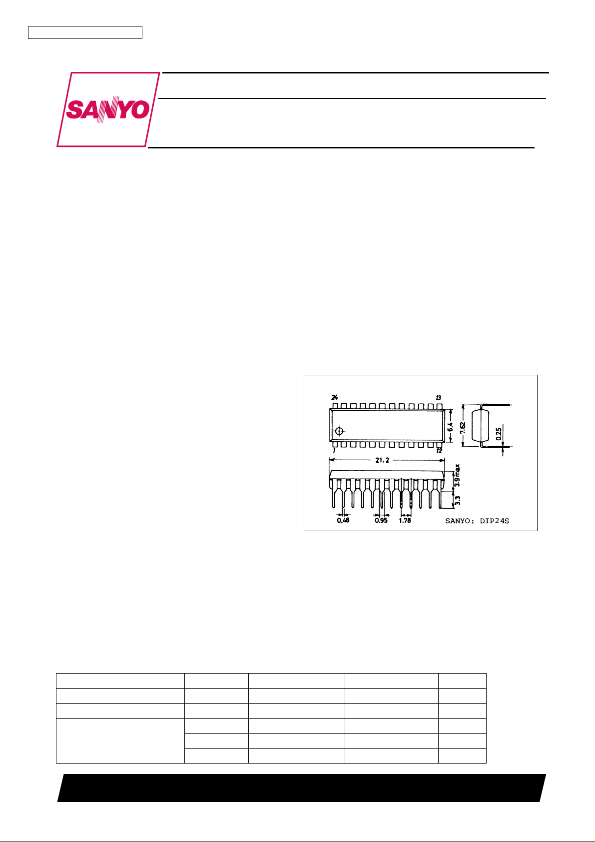
Package Dimensions
unit: mm
3067-DIP24S
[LA7577N]
1st SIF stage
• Preamplifier with AGC
• 1st SIF detector
SIF stage
• SIF limiter amplifier
• FM quadrature detector
Mute stage
• Sound mute (pin 2)
• AV mute (pin 4)
• IS-15 switch (pin 13)
Specifications
Absolute Maximum Ratings
Parameter Symbol Conditions Ratings Unit
Maximum supply voltage
Allowable power dissipation Pd max
Circuit voltages
at Ta = 25 ° C
V
max 13.8 V
CC
V
, V
3
V
11
V
23
Ta ≤ 50 ° C 1200 mW
13
V
CC
V
CC
V
CC
V
V
V
SANYO Electric Co., Ltd. Semiconductor Business Headquarters
TOKYO OFFICE Tokyo Bldg., 1-10, 1 Chome, Ueno, Taito-ku, TOKYO, 110 JAPAN
60597HA(ID) / 11795TH(ID) No. 4037—1/16
−
−
−
−
−
−
Parameter Symbol Conditions Ratings Unit
I
1
I
Circuit currents
1
Operating temperature range Topg V
17
I
21
I
22
I
10
CC
Storage temperature range Tstg
1. Current flowing into the IC is positive and current flowing out is negative.
LA7577N
= 9V, Ta = − 20 to +75 ° C
– −
−
∆
∆
−
−
1mA
10 mA
3mA
2mA
3mA
20 to +70 ° C
55 to +150 ° C
Recommended Operating Conditions
at Ta = 25 ° C
Parameter Symbol Ratings Unit
Supply voltage V
Operating supply voltage range V
Electrical Characteristics
at Ta = 25 ° C, V
CC
= 12V
CC
op 8.2 to 13.2 V
CC
9 or 12 V
Parameter Symbol Conditions min typ max Unit
[VIF]
Circuit current I
Quiescent video output voltage V
Maximum RF AGC voltage V
Minimum RF AGC voltage V
Quiescent AFT voltage V
Input sensitivity V
9
21
10H
10L
14
i
V
= 5V 44 55 68 mA
13
V
= 5V 6.6 7 7.4 V
13
V
= 7V 10.6 11 11.4 V
13
V
= 7V – 0 0.5 V
13
V
= 5V 3.0 5.9 8.0 V
13
33 39 45 dB/ µ V
AGC dynamic range GR 59 65 – dB
Maximum allowable input V
Video output amplitude V
max 100 105 – dB/ µ V
i
(video) 1.95 2.25 2.55 Vp-p
o
Output signal-to-noise ratio S/N 49 55 – dB
Sync signal tip voltage V
920kHz beat level l
Frequency characteristic f
Differential gain DG
Differential phase DP – 2 5 deg
Maximum AFT voltage V
Minimum AFT voltage V
White-noise threshold voltage V
White-noise clamp voltage V
Black-noise threshold voltage V
Black-noise clamp voltage V
AFT detector sensitivity S
VIF-stage input resistance R
VIF-stage input capacitance C
APC pull-in range (U) f
APC pull-in range (L) f
VCO maximum variation range
(tip) V
21
920
C
14H
14L
WTH
WCL
BTH
BCL
f
(VIF) f = 58.75MHz 0.8 1.3 1.75 k Ω
i
(VIF) f = 58.75MHz – 3.0 6.0 pF
i
PU-2
PL-2
f
U
f
L
= 10mV 4.15 4.45 4.75 V
i
P = 0, C = − 4dB, S = − 14dB 37 43 – dB
P = 0, S = − 14dB 6 8 – MHz
V
= 10mV, 87.5% mod,
i
f
= 58.75MHz
P
–36%
11 11.5 12 V
0 0.4 1.0 V
8.9 9.3 9.7 V
5.3 5.7 6.1 V
3.4 3.7 4.0 V
5.3 5.7 6.1 V
44 60 84 mV/kHz
0.6 1.6 – MHz
1.6
V
= 3V 0.6 1.6 – MHz
18
V
= 7V –
18
1.6
0.8 MHz
0.8 MHz
No. 4037—2/16
β
LA7577N
Parameter Symbol Conditions min typ max Unit
VCO control sensitivity
[1st SIF]
4.5MHz conversion gain VG 21 26 31 dB
4.5MHz output level V
1st SIF stage maximum input V
1st SIF stage input resistance R
1st SIF stage input capacitance C
SIF1
max +2.2dB, − 1dB 60 70 - mVrms
SIF
(SIF1) f = 54.25MHz 1.2 2 2.7 k Ω
i
(SIF1) f = 54.25MHz – 3 6 pF
i
[SIF]
SIF limiting sensitivity V
FM detector output voltage V
(lim) V
i
o
AM rejection AMR V
Total harmonic distortion THD V
SIF signal-to-noise ratio S/N (SIF) V
[Mute, Defeat]
AFT defeat start voltage V
AV mute threshold V
FM mute threshold V
AFT defeat voltage V
D11
4TH
2TH
D14
V
= 4.6 to 5V 1.5 3.1 6.2 kHz/mV
18
V
= 10mVrms 50 75 110 mVrms
i
= 5V – 33 39 dB/ µ V
13
V
= 5V 400 600 790 mVrms
13
= 5V 40 49 – dB
13
= 5V – 0.5 1.0 %
13
= 5V 60 78 – dB
13
0.5 2.3 – V
0.5 1.9 – V
0.5 2.0 – V
5.4 6 6.6 V
Electrical Characteristics
at Ta = 25 ° C, V
Parameter Symbol Conditions min typ max Unit
[VIF]
Circuit current I
Quiescent video output voltage V
Maximum RF AGC voltage V
Minimum RF AGC voltage V
Quiescent AFT voltage V
Input sensitivity V
Video output amplitude V
Sync signal tip voltage V
Maximum AFT voltage V
Minimum AFT voltage V
White-noise threshold voltage V
White-noise clamp voltage V
Black-noise threshold voltage V
Black-noise clamp voltage V
AFT detector sensitivity S
[SIF]
FM detector output voltage V
[Mute, Defeat]
AFT defeat start voltage V
AV mute threshold V
FM mute threshold V
AFT defeat voltage V
= 9V
CC
V
9
21
10H
10L
14
i
(video) 1.5 1.75 2.0 Vp-p
o
(tip) V
21
14H
14L
WTH
WCL
BTH
BCL
f
o
D11
4TH
2TH
D14
= 5V 39 48 59 mA
13
V
= 5V 5.0 5.4 5.8 V
13
V
= 7V 7.6 8 8.4 V
13
V
= 7V – 0 0.5 V
13
V
= 5V 2.6 4.5 6.0 V
13
37 43 49 dB/ µ V
= 10mV 3.25 3.55 3.85 V
i
8 8.5 9.0 V
– 0.3 1.0 V
6.8 7.2 7.6 V
4.0 4.4 4.8 V
2.5 2.8 3.1 V
2.5 4.1 4.5 V
28 39 55 mV/kHz
V
= 5V 400 600 790 mVrms
13
0.5 1.6 – V
0.5 1.1 – V
0.5 1.9 – V
3.9 4.5 5.1 V
No. 4037—3/16
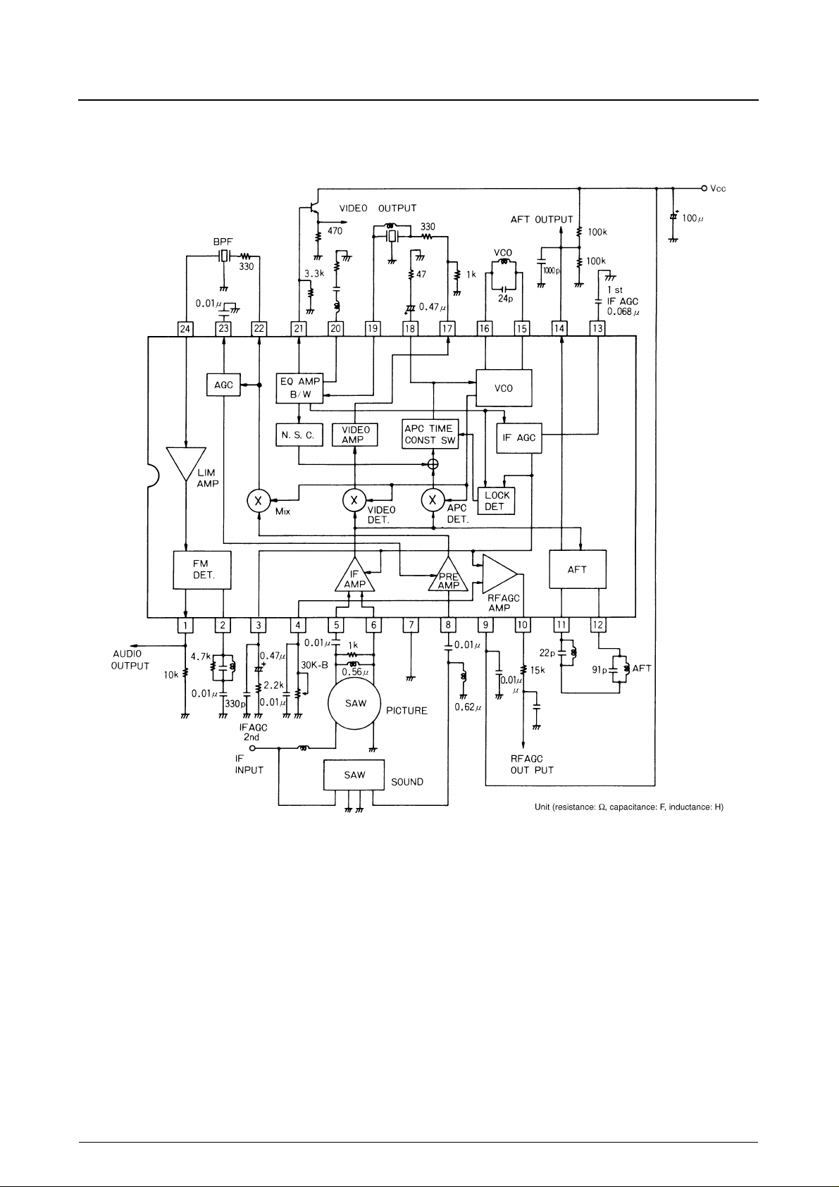
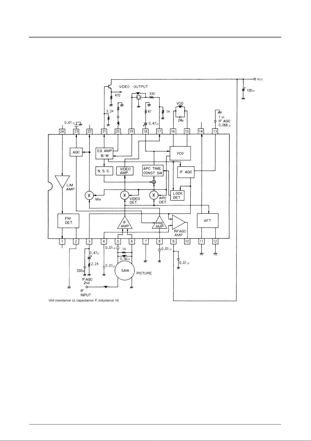
Sample Application Circuit (Japan)
LA7577N
No. 4037—4/16
LA7577N
Sample Application Circuit (Japan)
(when the SIF, 1st SIF, AFT and RF AGC are not used)
When the SIF stage is not used
• Leave pin 1 open
• Tie pin 2 to GND
• Leave pin 24 open
When the 1st SIF stage is not used
• Connect a 0.01µF capacitor between pin 8 and GND (leave the 0.01µF capacitor on pin 23 connected to GND)
• Leave pin 22 open
When the AFT circuit is not used
• Tie pins 11 and 12 to GND
• Leave pin 14 open
When the RF AGC circuit is not used
• Connect a 0.01µF capacitor between pin 4 and GND
• Leave pin 10 open
No. 4037—5/16
 Loading...