


Overview
The LA7567N and LA7567NM are PAL/NTSC multiformat audio VIF/SIF IF ICs that adopt a semiadjustment-free system. The VIF block adopts a technique
that makes AFT adjustment unnecessary by adjusting the
VCO, thus simplifying the adjustment steps in the
manufacturing process. PLL detection is adopted in the
FM detector to support multi-format audio detection. A
built-in SIF converter is included to simplify multi-format
system designs. A 5-V power-supply voltage is used to
match that used in most multimedia systems. In addition,
these ICs also include a buzz canceller to suppress Nyquist
buzz and provide high audio quality.
Functions
[VIF]
• VIF amplifier • PLL detector • BNC • RF AGC
• EQ amplifier • AFT • IF AGC • Buzz canceller
[First SIF]
• First SIF • First SIF detector • AGC
[SIF]
• Multi-format SIF converter • Limiter amplifier • PLL
FM detector
Features
• Both AFT and SIF inductors built in, thus making
adjustment of external inductance unnecessary.
• A PAL/NTSC multi-format audio system can be
constructed easily.
• Built-in buzz canceller for excellent audio performance.
•VCC= 5 V, low power dissipation (250 mW)
Package Dimensions
unit: mm
3067-DIP24S
unit: mm
3112-MFP24S
Monolithic Linear IC
50698RM (OT) No. 5765-1/14
SANYO: DIP24S
[LA7567N]
SANYO: MFP24S
[LA7567NM]
SANYO Electric Co.,Ltd. Semiconductor Bussiness Headquarters
TOKYO OFFICE Tokyo Bldg., 1-10, 1 Chome, Ueno, Taito-ku, TOKYO, 110-8534 JAPAN
TV and VCR VIF/SIF IF Signal-Processing Circuit with
PAL/NTSC Multi-Format Audio Support
LA7567N, 7567NM
Ordering number : EN5765
Parameter Symbol Conditions Ratings Unit
Maximum supply voltage V
CC
max 6V
Circuit voltage V13, V17 V
CC
V
I6 –3 mA
Circuit current I10 –10 mA
I24 –2 mA
TA ≤ 50°C, Independent IC [LA7567NM] 420 mW
Allowable power dissipation Pd max *: Mounted on a printed circuit board 720 mW
TA ≤ 70°C, Independent IC [LA7567N] 500 mW
Operating temperature Topr –20 to +70 °C
Storage temperature Tstg –55 to +150 °C
Specifications
Maximum Ratings at Ta = 25°C
Note: When mounted on a 65 × 72 × 1.6 mm paper/phenolic resin printed circuit board.
No. 5765-2/14
LA7567N, 7567NM
Parameter Symbol Conditions Ratings Unit
Recommended supply voltage V
CC
5 V
Operating supply voltage range V
CC
op 4.5 to 5.5 V
Operating Conditions at Ta = 25°C
Parameter Symbol Conditions
Ratings
Unit
min typ max
[VIF Block]
Circuit current I5 40.8 48.0 55.2 mA
Maximum RF AGC voltage V14H V
CC
– 0.5 V
CC
V
Minimum RF AGC voltage V14L 0 0.5 V
Input sensitivity V
IN
S1 = OFF 33 39 45 dBµV
AGC range G
R
58 63 dB
Maximum allowable input V
IN
max 95 100 dBµV
No-signal state video output voltage V6 3.0 3.3 3.6 V
Synchronizing signal tip voltage V6 tip 1.15 1.45 1.74 V
Video output level V
O
1.36 1.60 1.84 Vp-p
Black noise threshold voltage V
BTH
0.5 0.8 1.1 V
Black noise clamp voltage V
BCL
1.6 1.9 2.2 V
Video signal-to-noise ratio S/N 48 52 dB
C-S beat IC-S 38 43 dB
Frequency characteristics f
C
6 MHz –3.0 –1.5 dB
Differential gain DG 3.0 6.5 %
Differential phase DP 3 5 deg
No-signal state AFT voltage V13 2.0 2.5 3.0 V
Maximum AFT voltage V13H 4.0 4.4 5.0 V
Minimum AFT voltage V13L 0 0.18 1.00 V
AFT detection sensitivity Sf 20 28 37 mV/kHz
VIF input resistance Ri 38.9 MHz 1.5 kΩ
VIF input capacitance Ci 38.9 MHz 3 pF
APC pull-in range (U) f
PU
0.7 1.5 MHz
APC pull-in range (L) f
PL
–1.5 –0.9 MHz
AFT tolerance frequency 1 dfa1 –300 0 +300 kHz
VCO1 maximum variability range (U) dfu 1.0 1.5 MHz
VCO1 maximum variability range (L) dfl –1.5 –1.0 MHz
VCO control sensitivity B 1.4 2.8 6.0 kHz/mV
[First SIF Block]
Conversion gain VG 22 28 32 dB
5.5 MHz output level S
O
32 70 110 mVrms
First SIF maximum input S
IN
max 50 100 mVrms
First SIF input resistance R
IN
(SIF) 33.4 MHz 2 kΩ
First SIF input capacitance C
IN
(SIF) 33.4 MHz 3 pF
[SIF Block]
Limiting sensitivity Vli (lim) 42 48 54 dBµV
FM detector output voltage V
O
(FM) 5.5 MHz ±30 kHz * 480 680 880 mVrms
AMR rejection ratio AMR 50 60 dB
Total harmonic distortion THD 0.3 0.8 %
SIF S/N S/N (FM) 57 62
[SIF Converter]
Conversion gain VG (SIF) 8 11 14 dB
Maximum output level V max 103 109 115 dBµV
Carrier suppression ratio VGR (5.5) 15 21 dB
Oscillator level V
OSC
35 70 mVp-p
Oscillator leakage OSCleak 14 25 dB
Oscillator stopped current I
4
300 µA
Operating Characteristics at Ta = 25°C, VCC= 5 V, fp = 38.9 MHz
Note: *Insert a resistor and capacitor in series between pin 23 and ground to adjust the level to acquire a wide dynamic range in the FM detector output.
Pin Assignment
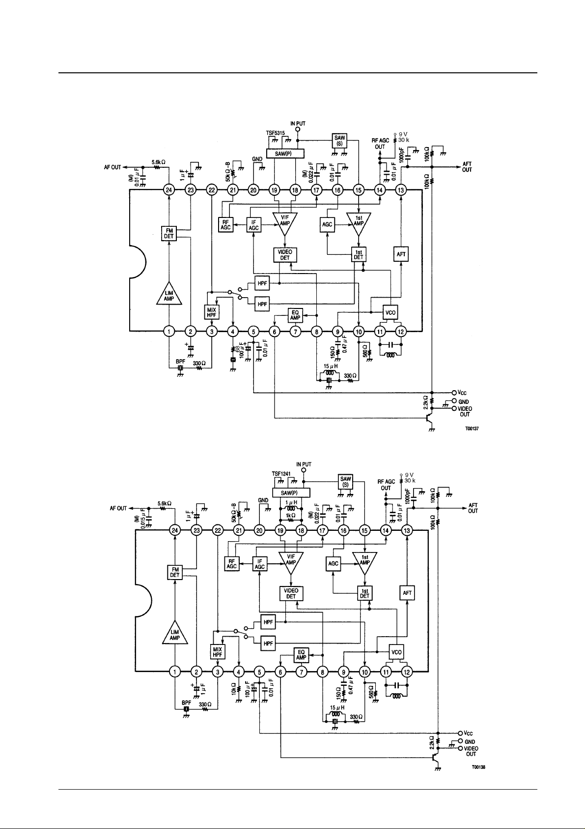
Internal Equivalent Circuit and External Components
No. 5765-3/14
LA7567N, 7567NM
Allowable power dissipation, Pd max — W
Ambient temperature, Ta — °C
AC Characteristics Test Circuit
Test Circuit
No. 5765-4/14
LA7567N, 7567NM
Impedance
analyzer
No. 5765-5/14
LA7567N, 7567NM
Application Circuit Diagrams
PAL SPLIT
NT (US) SPLIT