

Sanyo LA7567GM Specifications
Any and all SANYO products described or contained herein do not have specifications that can handle
applications that require extremely high levels of reliability, such as life-support systems, aircraft’s
control systems, or other applications whose failure can be reasonably expected to result in serious
physical and/or material damage. Consult with your SANYO representative nearest you before using
any SANYO products described or contained herein in such applications.
SANYO assumes no responsibility for equipment failures that result from using products at values that
exceed, even momentarily, rated values (such as maximum ratings, operating condition ranges, or other
parameters) listed in products specifications of any and all SANYO products described or contained
herein.
Overview
The LA7567GM is an NTSC SPLIT support VIF/SIF IF
IC that adopts a semi-adjustment-free system. The VIF
block adopts a technique that makes AFT adjustment
unnecessary by adjusting the VCO, thus simplifying the
adjustment steps in the manufacturing process. PLL
detection is adopted in the FM detector. A 5-V powersupply voltage is used to match that used in most
multimedia systems. In addition, this IC also includes a
buzz canceller to suppress Nyquist buzz and provide high
audio quality.
Functions
[VIF]
• VIF amplifier • PLL detector • BNC • RF AGC
• EQ amplifier • AFT • IF AGC • Buzz canceller
[First SIF]
• First SIF • First SIF detector • AGC
[SIF]
• Multi-format SIF converter • Limiter amplifier • PLL
FM detector
Features
• Both AFT and SIF inductors built in, thus making
adjustment of external inductance unnecessary.
• Built-in buzz canceller for excellent audio performance.
•VCC= 5 V, low power dissipation (250 mW)
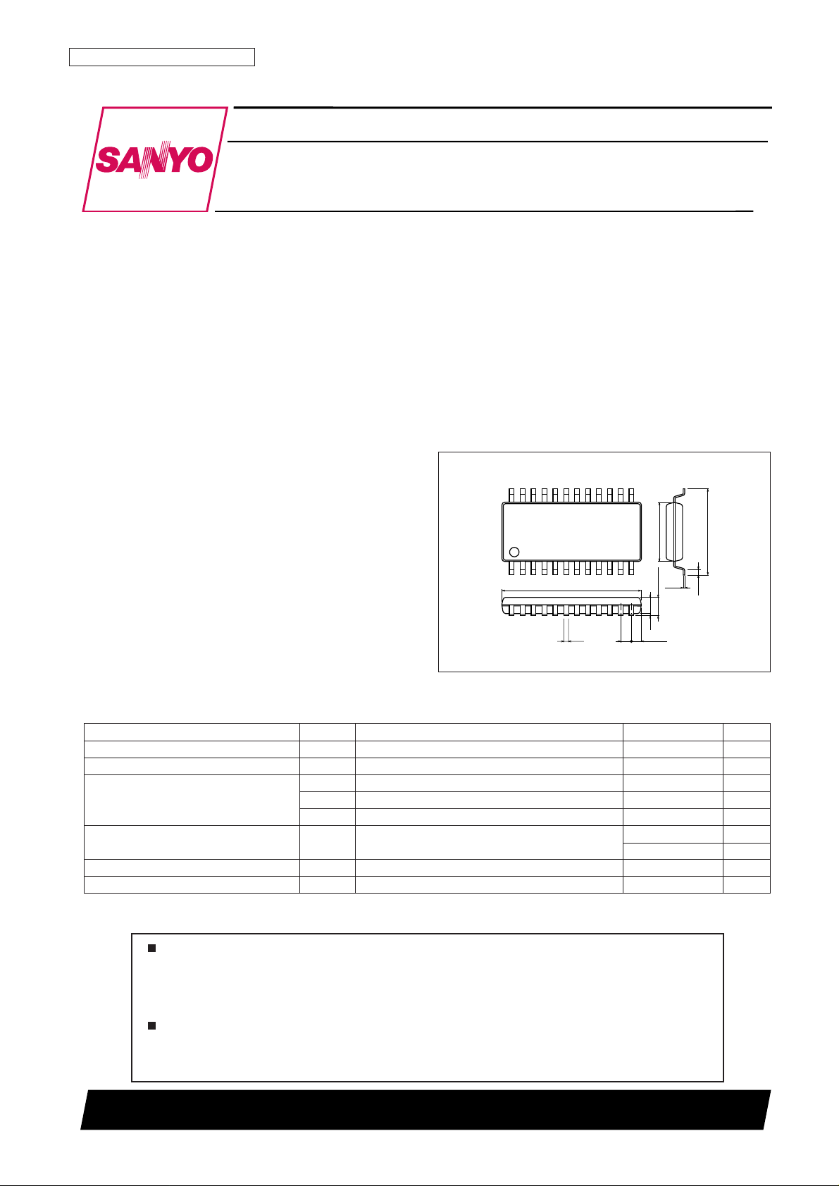
Package Dimensions
unit: mm
3112A-MFP24S
Monolithic Linear IC
D1401RM (OT) No. 6803-1/14
112
24
13
12.5
(0.75)
1.0
0.15
0.35
5.4
7.6
0.63
1.7max
1.5
0.1
SANYO: MFP24S
[LA7567GM]
SANYO Electric Co.,Ltd. Semiconductor Company
TOKYO OFFICE Tokyo Bldg., 1-10, 1 Chome, Ueno, Taito-ku, TOKYO, 110-8534 JAPAN
TV and VCR VIF/SIF IF Signal-Processing Circuit with
NTSC SPLIT Support
LA7567GM
Ordering number : ENN6803
Parameter Symbol Conditions Ratings Unit
Maximum supply voltage V
CC
max 6V
Circuit voltage V13, V17 V
CC
V
I6 –3 mA
Circuit current I10 –10 mA
I24 –2 mA
Allowable power dissipation Pd max
TA ≤ 50°C, Independent IC
420 mW
*: Mounted on a printed circuit board
720 mW
Operating temperature Topr –20 to +70 °C
Storage temperature Tstg –55 to +150 °C
Specifications
Maximum Ratings at Ta = 25°C
Note: When mounted on a 65 × 72 × 1.6 mm paper/phenolic resin printed circuit board.
No. 6803-2/14
LA7567GM
Parameter Symbol Conditions Ratings Unit
Recommended supply voltage V
CC
5 V
Operating supply voltage range V
CC
op 4.5 to 5.5 V
Operating Conditions at Ta = 25°C
Parameter Symbol Conditions
Ratings
Unit
min typ max
[VIF Block]
Circuit current I5 40 47.5 54.5 mA
Maximum RF AGC voltage V14H V
CC
– 0.5 V
CC
V
Minimum RF AGC voltage V14L 0 0.5 V
Input sensitivity V
IN
S1 = OFF 27 33 39 dBµV
AGC range G
R
53 58 dB
Maximum allowable input V
IN
max 90 96 dBµV
No-signal state video output voltage V6 2.1 2.4 2.7 V
Synchronizing signal tip voltage V6 tip 0.7 1.0 1.3 V
Video output level V
O
0.95 1.1 1.25 Vp-p
Black noise threshold voltage V
BTH
0.5 0.8 1.1 V
Black noise clamp voltage V
BCL
1.2 1.5 1.8 V
Video signal-to-noise ratio S/N 48 52 dB
C-S beat IC-S 38 43 dB
Frequency characteristics f
C
6 MHz –3.0 –1.5 dB
Differential gain DG 3.0 6.5 %
Differential phase DP 3 5 deg
No-signal state AFT voltage V13 2.0 2.5 3.0 V
Maximum AFT voltage V13H 4.0 4.4 5.0 V
Minimum AFT voltage V13L 0 0.18 1.00 V
AFT detection sensitivity Sf 14 21 28 mV/kHz
VIF input resistance R
IN
45.75 MHz 1.5 kΩ
VIF input capacitance C
IN
45.75 MHz 3 pF
APC pull-in range (U) f
PU
0.7 1.5 MHz
APC pull-in range (L) f
PL
–2.0 –1.4 MHz
AFT tolerance frequency 1 dfa1 –200 0 +200 kHz
VCO1 maximum variability range (U) dfu 1.0 1.5 MHz
VCO1 maximum variability range (L) dfl –2.0 –1.4 MHz
VCO control sensitivity B 1.2 3.2 5.0 kHz/mV
Sync ratio VS 25.0 28.5 31.5 %
[First SIF Block]
Conversion gain VG 27 33 39 dB
4.5 MHz output level S
O
53 115 180 mVrms
First SIF maximum input S
IN
max 8 16 mVrms
First SIF input resistance R
IN
(SIF) 41.25 MHz 2 kΩ
First SIF input capacitance C
IN
(SIF) 41.25 MHz 3 pF
[SIF Block]
Limiting sensitivity Vli (lim) 44 50 56 dBµV
FM detector output voltage V
O
(FM) 4.5 MHz ±25 kHz * 350 450 570 mVrms
AMR rejection ratio AMR 50 60 dB
Total harmonic distortion THD 0.3 0.8 %
SIF S/N S/N (FM) 59 65
[SIF Converter]
Maximum output level V max 110 116 122 dBµV
Electrical Characteristics at Ta = 25°C, VCC= 5.0 V, fp = 45.75 MHz
Note: *The FM detector output level can be reduced and the FM dynamic range can be increased by inserting a resistor and a capacitor in series between
pin 23 and ground.
Pin Assignment
Internal Equivalent Circuit and External Components
No. 6803-3/14
LA7567GM
1
2
3
4
5
6
7
8
9
10
11
12 13
14
15
16
17
18
19
20
21
22
23
24
2nd SIF INPUT
BIAS FILTER
MIX OUT
CER.OSC
V
CC
VIDEO OUT
EQ FILTER
EQ INPUT
APC FILTER
VIDEO DET OUT
VCO COIL
VCO COIL AFT OUT
RF AGC OUT
1st SIF INPUT
1st SIF AGC FILTER
IF AGC FILTER
VIF
VIF
GND
RF AGC VR
1st SIF OUT
(NICAM OUT)
FM FILTER
FM DET OUT
A13679
LA7567GM
Top view
SAW(P
)
+
+
+
VCO
COIL
100k
Ω
100k
Ω
7.5k
Ω
330
Ω
150
Ω
3k
Ω
330
Ω
10k
Ω
10k
Ω
-
B
300
Ω
1k
Ω
30pF
620
Ω
1k
Ω
1k
Ω
400
Ω
400
Ω
1k
Ω
30k
Ω
1k
Ω
1k
Ω
1k
Ω
1k
Ω
10k
Ω
2k
Ω
2k
Ω
1k
Ω
100
Ω
2k
Ω
6k
Ω
500
Ω
3.3k
Ω
200
Ω
9.2k
Ω
1.2kΩ1.2k
Ω
1k
Ω
1kΩ1k
Ω
2k
Ω
200
Ω
10k
Ω
18k
Ω
SAW
(S)
24 23 22 21 20 19 18 17 16 15 14 13
1 2 3 4 5 6 7 8 9 10 11 12
100
µ
F
0.47
µ
F
0.47 to 1
µ
F
0.01
µ
F
VIDEO
OUT
0.01
µ
F
0.01
µ
F
1
µ
F
0.022
µ
F
0.01
µ
F
0.01
µ
F
0.01
µ
F
AUDIO
OUTPUT
RFAGC
VR
RF AGC
OUTPUT
IF
9V
IN PUT
GND
BPF
AFT
OUTPUT
V
CC
V
V
V
1V
6MHz
T00134
Allowable power dissipation, Pd max — W
Ambient temperature, Ta — °C
0
80 10060 704020-20 0
Pdmax — Ta
200
100
400
300
600
500
800
700
720
420
Independent IC
Mounted on a printed circuit board
AC Characteristics Test Circuit
Test Circuit
No. 6803-4/14
LA7567GM
+
+
+
+
100k
Ω
100k
Ω
30k
Ω
100k
Ω
1.5k
Ω
7.5k
Ω
330
Ω
560
Ω
10k
Ω
10k
Ω
150
Ω
51
Ω
10k
Ω
-
B
51
Ω
51
Ω
FM
DET
RF
AGC
IF
AGC
AGC
1st
DET
VCO
EQ
AMP
MIX
HPF
HPF
VIDEO
DET
HPF
AFT
LIM
AMP
VIF
AMP
24 23 22 21 20 19 18 17 16 15 14 13
1 2 3 4 5 6 7 8 9 10 11 12
1st
AMP
1
µ
F
0.01
µ
F
0.47
µ
F
0.01
µ
F
1
µ
F
(
M
)
(D)
(A)
(E)
0.01
µ
F
0.01
µ
F
0.01
µ
F
0.01
µ
F
0.01
µ
F
0.01
µ
F
0.01
µ
F
0.01
µ
F
1000pF
24pF
(
M
)
(F)
(B)
FM DET OUT
GND
IF AGC
1st SIF IN
2nd SIF IN
CONV.OUT
VIDEO
OUT
VIFIN
RF AGC
9V
OUT
V
CC
GND
AFT
OUT
T00135
RF AGC
V
R
1st SIF OUT
(
NICAM OUT
)
S2
S1
+
100kΩ100k
Ω
10k
Ω
330
Ω
10k
Ω
24 23 22 21 20 19 18 17 16 15 14 13
1 2 3 4 5 6 7 8 9 10 11 12
100
µ
F
0.01
µ
F
0.01
µ
F
0.01
µ
F
0.01
µ
F
0.01
µ
F
0.01
µ
F
0.01
µ
F
0.01
µ
F
0.01
µ
F
0.01
µ
F
0.01
µ
F
0.01
µ
F
V
CC
T00136
1st SIF IN
VIFIN
Impedance
analyzer
LA7567GM
No. 6803-5/14
LA7567GM
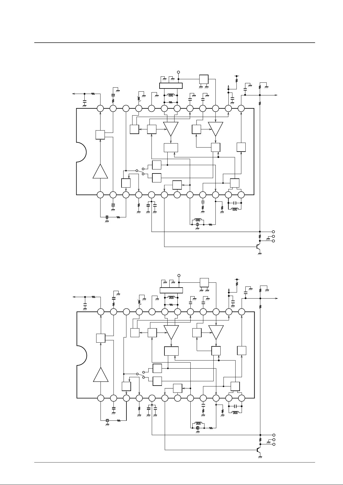
Application Circuit Diagrams
NT (US) SPLIT
+
+
2.2k
Ω
100k
Ω
100k
Ω
1k
Ω
7.5k
Ω
330
Ω
560
Ω
10k
Ω
150
Ω
330
Ω
10k
Ω
-
B
FM
DET
SAW
(S)
RF
AGC
IF
AGC
AGC
1st
DET
VCO
EQ
AMP
MIX
HPF
HPF
VIDEO
DET
SAW(P
)
HPF
AFT
LIM
AMP
VIF
AMP
24 23 22 21 20 19 18 17 16 15 14 13
1 2 3 4 5 6 7 8 9 10 11 12
1st
AMP
100
µ
F
1
µ
F
0.01
µ
F
15µH
0.47
µ
F
0.01
µ
F
(
M
)
0.022
µ
F
1µH
0.01
µ
F
0.01
µ
F
1000pF
(
M
)
AF OUT
GND
TSF1241
IN PUT
RF AGC
OUT
GND
VIDEO
OUT
BPF
AFT
OUT
V
CC
T00138
+
1
µ
F
30k
Ω
9V
JAPAN SPLIT
+
+
+
1
µ
F
2.2k
Ω
100k
Ω
100k
Ω
1k
Ω
7.5k
Ω
330
Ω
560
Ω
10k
Ω
150
Ω
330
Ω
10k
Ω
-
B
FM
DET
SAW
(S)
RF
AGC
IF
AGC
AGC
1st
DET
VCO
EQ
AMP
MIX
HPF
HPF
VIDEO
DET
SAW(P
)
HPF
AFT
LIM
AMP
VIF
AMP
24 23 22 21 20 19 18 17 16 15 14 13
1 2 3 4 5 6 7 8 9 10 11 12
1st
AMP
100
µ
F
1
µ
F
0.01
µ
F
15µH
0.47
µ
F
0.01
µ
F
(
M
)
0.022
µ
F
0.01
µ
F
0.01
µ
F
1000pF
(
M
)
AF OUT
GND
TSF1137
IN PUT
RF AGC
OUT
GND
VIDEO
OUT
BPF
AFT
OUT
V
CC
T00139
30k
Ω
9V
 Loading...