

Sanyo LA75675M-S Specifications
Ordering number : ENN6276B
51500RM (OT) No. 6276-1/13
Overview
The LA75675M-S is an NTSC intercarrier VIF/SIF IC
that adopts a semi-adjustment-free structure. In particular,
it uses VCO adjustment to make AFT adjustment
unnecessary and thus simplifies the overall adjustment
process. A PLL-based technique is adopted for FM
detection. The 5 V supply voltage provides compatibility
with other multimedia systems. In addition it achieves
high audio quality by incorporating a built-in buzz
canceller that suppresses Nyquist buzz.
Functions
[VIF]
• VIF amplifier • PLL detector • BNC • RF AGC
• EQ amplifier • AFT • IF AGC • Buzz canceller
[SIF]
• Limiter amplifier • PLL FM detector
Features
• No AFT or SIF coils are used, thus eliminating
adjustments.
• Excellent audio performance due to the built-in buzz
canceller.
•VCC= 5 V and a low power dissipation of 250 mW.
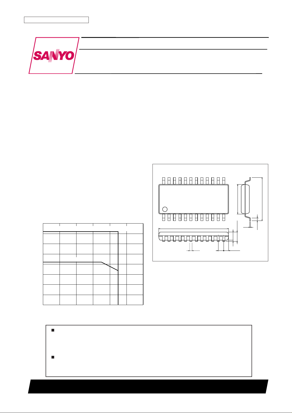
Package Dimensions
unit: mm
3112A-MFP24S
112
24
13
12.5
(0.75)
1.0
0.15
0.35
5.4
7.6
0.63
1.7max
1.5
0.1
SANYO: MFP24S
[LA75675M-S]
LA75675M-S
SANYO Electric Co.,Ltd. Semiconductor Company
TOKYO OFFICE Tokyo Bldg., 1-10, 1 Chome, Ueno, Taito-ku, TOKYO, 110-8534 JAPAN
VIF/SIF IF Signal-Processing Circuit that Supports
NTSC Intercarrier for TV and VCR Products
Monolithic Linear IC
Any and all SANYO products described or contained herein do not have specifications that can handle
applications that require extremely high levels of reliability, such as life-support systems, aircraft’s
control systems, or other applications whose failure can be reasonably expected to result in serious
physical and/or material damage. Consult with your SANYO representative nearest you before using
any SANYO products described or contained herein in such applications.
SANYO assumes no responsibility for equipment failures that result from using products at values that
exceed, even momentarily, rated values (such as maximum ratings, operating condition ranges, or other
parameters) listed in products specifications of any and all SANYO products described or contained
herein.
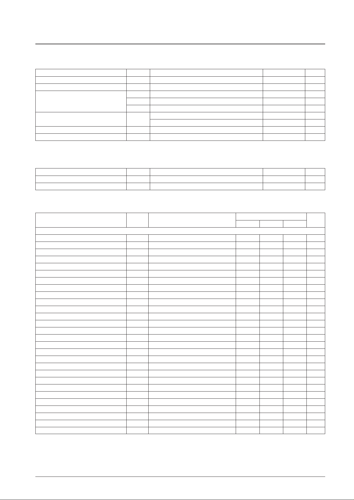
Independent IC
When mounted on a 65 × 72 × 1.6 mm3 paper-phenol printed circuit board
0
80 10060 704020-20 0
Ambient temperature, Ta — °C
Allowable power dissipation, Pdmax — W
Pdmax
-
Ta
200
100
400
300
600
500
800
700
720
420
No. 6276-2/13
LA75675M-S
Parameter Symbol Conditions Ratings Unit
Maximum supply voltage V
CC
max 6V
Circuit voltage V13, V17 V
CC
V
I6 –3 mA
Circuit current I10 –10 mA
I24 –2 mA
Allowable power dissipation Pd max
Ta ≤ 50°C, independent IC 420 mW
*: Mounted on a PCB. 720 mW
Operating temperature Topr –20 to +70 °C
Storage temperature Tstg –55 to +150 °C
Specifications
Maximum Ratings at Ta = 25°C
*: A 65 × 72 × 1.6 mm3paper-phenol printed circuit board
Parameter Symbol Conditions Ratings Unit
Recommended supply voltage V
CC
5V
Operating voltage range V
CC
op 4.5 to 5.5 V
Operating Conditions at Ta = 25°C
Parameter Symbol Conditions
Ratings
Unit
min typ max
[VIF Block]
Circuit current I5 32 40 48 mA
Maximum RF AGC voltage V14H VCC– 0.5 V
CC
V
Minimum RF AGC voltage V14L 0 0.5 V
Input sensitivity V
IN
S1 = OFF 32 38 44 dBµV
AGC range G
R
58 63 dB
Maximum allowable input V
IN
max 95 100 dBµV
No-signal video output voltage V6 3.5 3.8 4.1 V
Sync signal tip voltage V6 tip 0.9 1.2 1.5 V
Video output level V
O
1.7 2.0 2.3 Vp-p
Black noise threshold voltage V
BTH
0.5 0.8 1.1 V
Black noise clamp voltage V
BCL
1.6 1.9 2.2 V
Video signal-to-noise ratio S/N 48 52 dB
C-S beating IC-S 38 43 dB
Frequency characteristics f
C
6 MHz –3.0 –1.5 dB
Differential gain DG 3.0 6.5 %
Differential phase DP 3 5 deg
No-signal AFT voltage V13 2.0 2.5 3.0 V
Maximum AFT voltage V13H 4.0 4.4 5.0 V
Minimum AFT voltage V13L 0 0.18 1.00 V
AFT detection sensitivity Sf 28 40 52 mV/kHz
VIF input resistance R
IN
45.75 MHz 1.5 kΩ
VIF input capacitance C
IN
45.75 MHz 3 pF
APC pull-in range (U) f
PU
1.3 2.0 MHz
APC pull-in range (L) f –2.0 –1.4 MHz
AFT tolerance frequency 1 dfa 1 –150 0 +150 kHz
VCO 1 maximum variability range (U) dfu 1.5 2.0 MHz
VCO 1 maximum variability range (L) dfl –2.0 –1.5 MHz
VCO control sensitivity B 1.3 2.7 5.4 kHz/mV
Electrical Characteristics at Ta = 25°C, VCC= 5.0 V, fp = 45.75 MHz
Continued on next page.
No. 6276-3/13
LA75675M-S
Continued from preceding page.
Note: 1. The FM detection output level can be reduced and the FM dynamic range improved by inserting the resistor R in series with the capacitor between
pin 23 and ground.
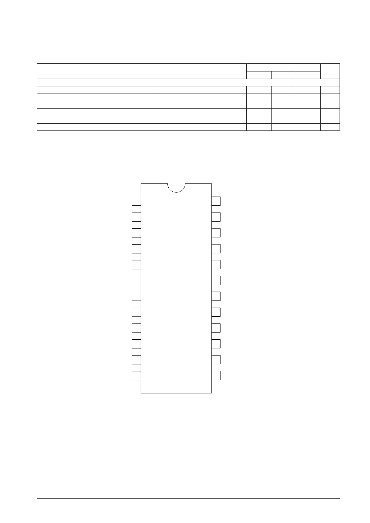
Pin Arrangement
Parameter Symbol Conditions
Ratings
Unit
min typ max
[SIF Block]
Limiting sensitivity Vli (lim) 39 45 51 dBµV
FM detection output voltage VO(FM) 4.5 MHz ± 25 kHz *
1
400 520 660 mVrms
AMR rejection ratio AMR 50 60 dB
Total harmonic distortion THD 0.3 0.8 %
SIF signal-to-noise ratio S/N (FM) 59 64 dB
4.5 MHz output level Vsout SIF IN 80 dBµV 82 89 96 dBµV
SIF INPUT
BIAS FILTER
SIF OUT
1
2
3
24
FM DET OUT
23
FM FILTER
22
BPF-OUT
4
NC
5
V
CC
VIDEO OUT
6
LA75675M-S
EQ FILTER
EQ INPUT
APC FILTER
VIDEO DET OUT
VCO COIL
VCO COIL AFT OUT
7
8
9
10
11
12 13
21
RF AGC VR
20
GND
19
VIF INPUT
18
VIF INPUT
17
1st AGC FILTER
16
2nd AGC FILTER
15
2nd AGC FILTER
14
RF AGC OUT
Top view
A12615
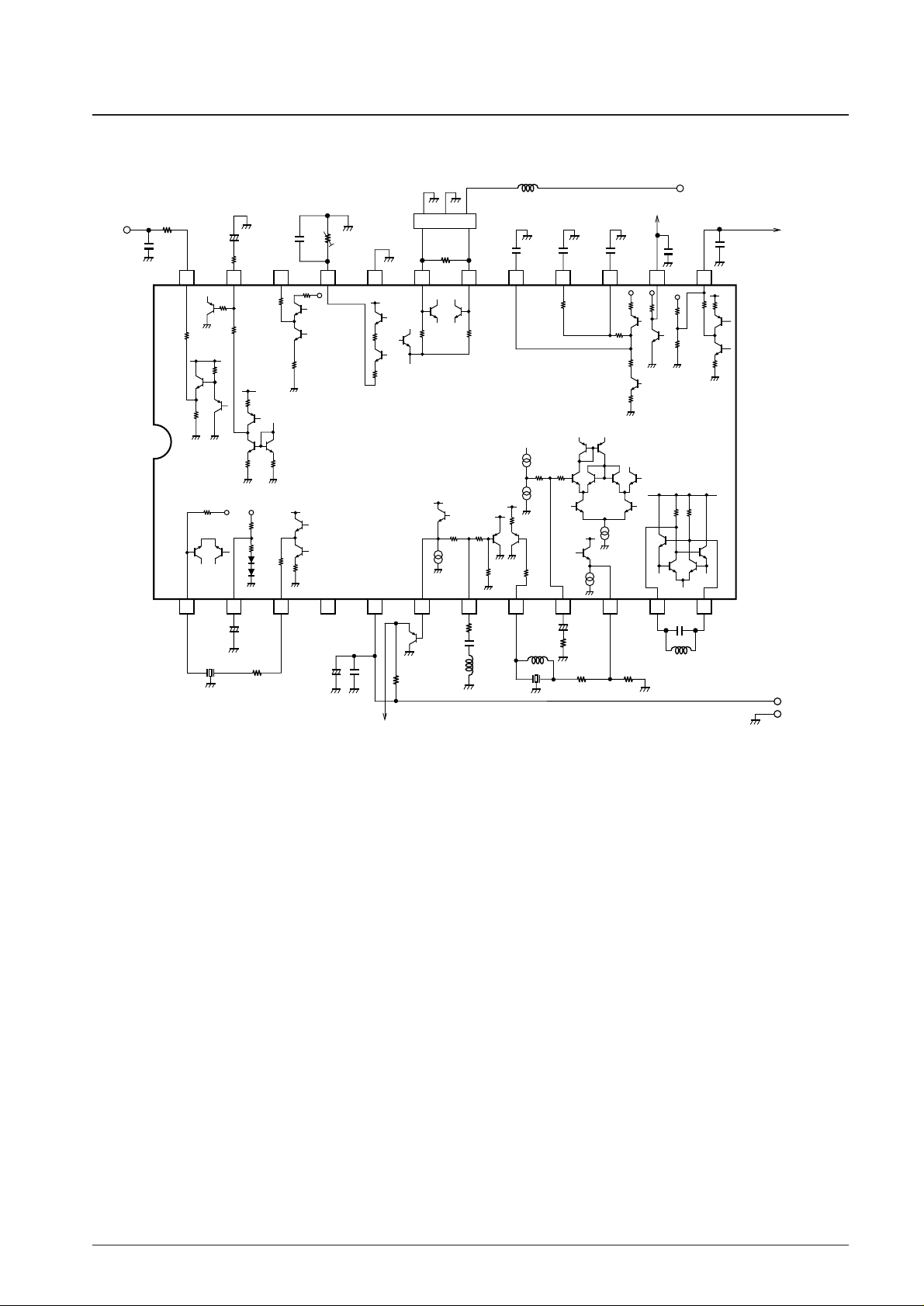
Internal Equivalent Circuit and External Circuits
No. 6276-4/13
LA75675M-S
SAW(P
)
+
+
+
VCO
COIL
R
7.5 k
Ω
330
Ω
150
Ω
2.2 k
Ω
330
Ω
10 k
Ω
-
B
300
Ω
1 k
Ω
1 k
Ω
1 k
Ω
1 k
Ω
1 k
Ω
1 k
Ω
120 k
Ω
120 k
Ω
6.8 k
Ω
2 k
Ω
30 k
Ω
1 k
Ω
10 k
Ω
500
Ω
100
Ω
10 k
Ω
200
Ω
9.2 k
Ω
1.2 k
Ω
1.2 k
Ω
1 k
Ω
1 k
Ω
1 k
Ω
4.7 k
Ω
2.2 k
Ω
200
Ω
10 k
Ω
4 k
Ω
24 23 22 21 20 19 18 17 16 15 14 13
123456789101112
1
µ
F
0.47
µ
F
1
µ
F
0.01
µ
F
VIDEO
OUT
0.01
µ
F
0.01
µ
F
1
µ
F
0.015
µ
F
0.01
µ
F
330 pF
0.01
µ
F
0.01
µ
F
AUDIO
OUTPUT
RFAGC
VR
RF AGC
OUTPUT
IF
IN PUT
GND
BPF
AFT
OUTPUT
V
CC
V
V
V
V
1 V
4.5 MHz
A12616
Note: Resistor R must have a value of 470 Ω or larger.
 Loading...