

SANYO LA7565BM, LA7565B Datasheet
Ordering number :EN5636
83097HA(OT) No. 5636-1/16
Overview
The LA7565B/M is a PAL/NTSC multi-system audio
VIF/SIF signal-processing IC that adopts a minimaladjustment technique. The VIF circuit adopts a minimaladjustment technique in which AFT adjustment is made
unnecessary by VCO adjustment to simply end product
adjustment. The FM detector circuit uses PLL detections
to support multi-system audio detection. Since the
LA7565BM include an SIF converter on chip, it is easy to
implement multi-system audio. In addition, it also includes
a buzz canceller that suppresses Nyquist buzz to achieve
improved audio quality.
Functions
[VIF Block]
• Minimal adjustment PLL detector
• AFT
• RF AGC
• Equalizer amplifier
• SIF converter
[First SIF Block]
• First SIF detector
• Inter/split switch
• HPF
[SIF Block]
• PLL type FM detector
[Mute Block]
• AV mute
Features
• Allows the use of a switch circuit to switch between
spilt and intercarrier operation.
• Improved buzz and buzz beat characteristics provided by
a PLL detector plus buzz canceller system.
• The IF AGC second filter is built in.
• PAL/NTSC multi-system audio can be implemented
easily.
• Adjustment-free circuit design that does not require AFT
and SIF coils.
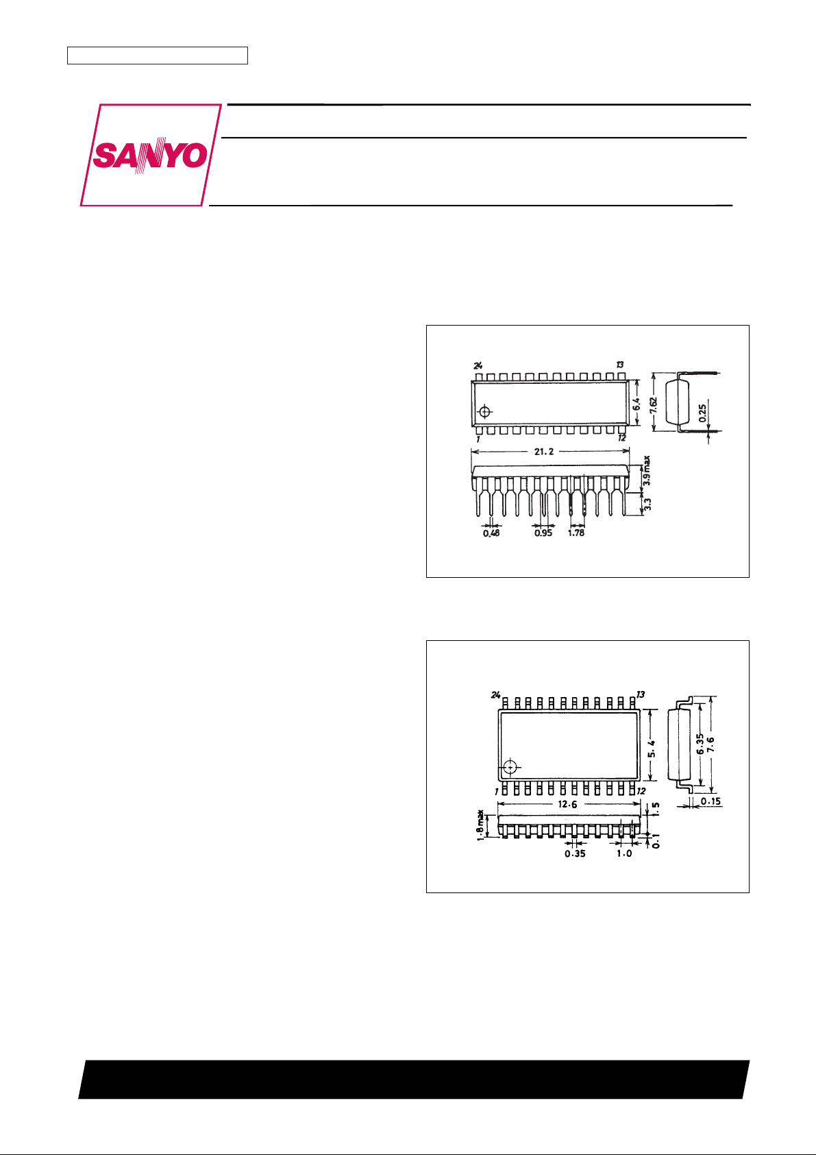
Package Dimensions
unit: mm
3067-DIP24S
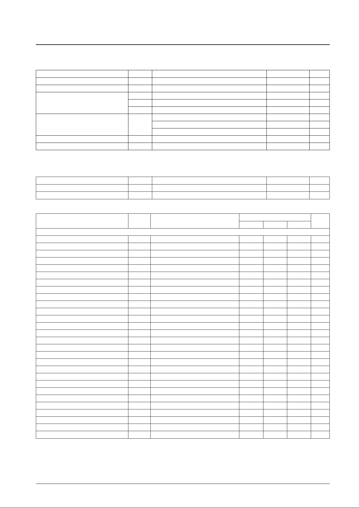
unit: mm
3112-MFP24S
SANYO: DIP24S
[LA7565B]
SANYO: MFP24S
[LA7565BM]
LA7565B, 7565BM
SANYO Electric Co.,Ltd. Semiconductor Bussiness Headquarters
TOKYO OFFICE Tokyo Bldg., 1-10, 1 Chome, Ueno, Taito-ku, TOKYO, 110 JAPAN
IF Signal-Processing IC for PAL/NTSC Multi-System
Audio TV and VCR Products
Monolithic Linear IC
No. 5636-2/16
LA7565B, 7565BM
Parameter Symbol Conditions Ratings Unit
Maximum supply voltage V
CC
max 10 V
Circuit voltage V13, V17 V
CC
V
I6 –3 mA
Circuit current I10 –10 mA
I24 –2 mA
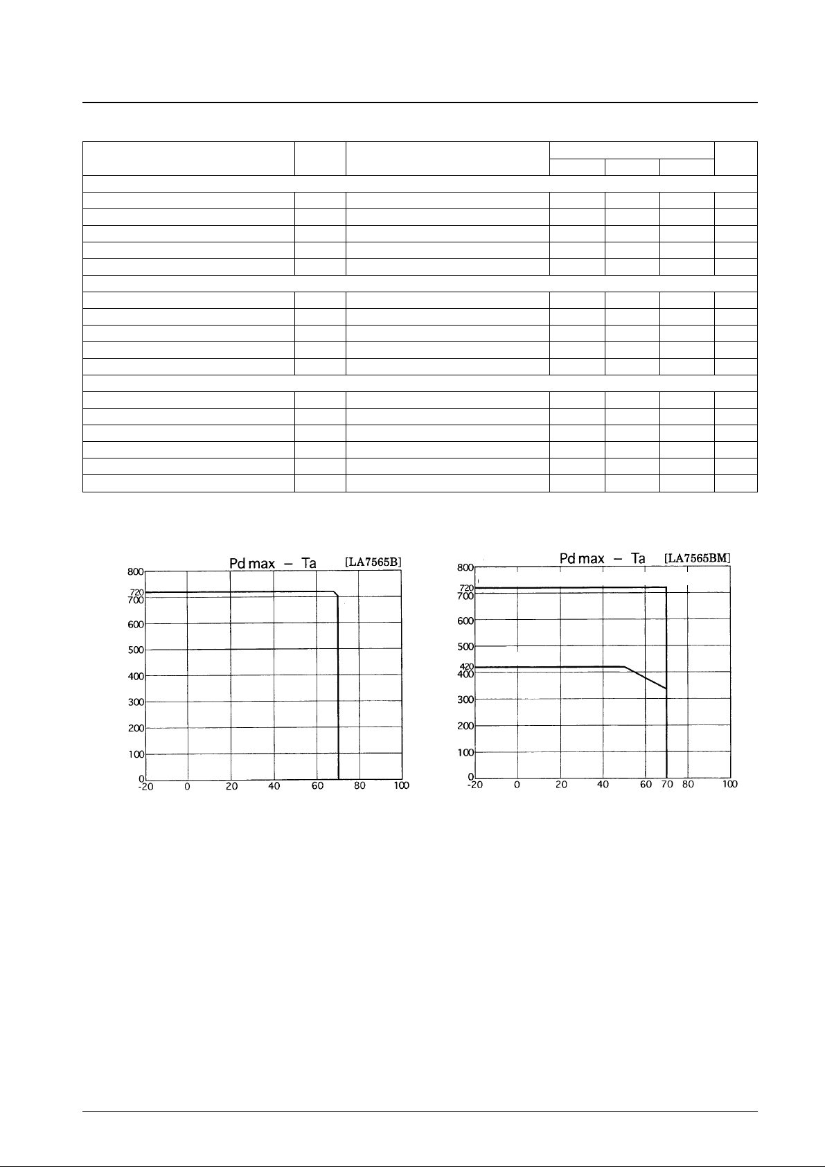
(LA7565B) Ta ≤ 68°C 720 mW
Allowable power dissipation Pd max (LA7565BM) Ta ≤ 50°C, independent IC 420 mW
(LA7565BM) * Mounted on a printed circuit board 720 mW
Operating temperature Topr –20 to +70 °C
Storage temperature Tstg –55 to +150 °C
Specifications
Maximum Rating at Ta = 25°C
Parameter Symbol Conditions Ratings Unit
Recommended supply voltage V
CC
9 V
Operating supply voltage V
CC
op 8.5 to 9.5 V
Operating Conditions
Note: * When mounted on a 65 × 72 × 1.6 mm epoxy glass laminate printed circuit board.
Parameter Symbol Conditions
Ratings
Unit
min typ max
[VIF Block]
Circuit current I
5
37.4 44 50.6 mA
Maximum RF AGC voltage V
14H
7.5 8.1 V
Minimum RF AGC voltage V
14L
0 0.5 V
Input sensitivity V
IN
S1 = OFF 26 32 38 dBµV
AGC range G
R
62 68 dB
Maximum allowable input V
IN
max 92 97 dBµV
No-signal video output voltage V
6
3.5 3.8 4.2 V
Synchronizing signal tip voltage V
6
tip 1.15 1.45 1.74 V
Video output level V
O
1.7 2.0 2.3 Vp-p
Black noise threshold voltage V
BTH
0.5 0.8 1.1 V
Black noise clamp voltage V
BCL
2.5 2.8 3.1 V
Video S/N ratio S/N 48 50 dB
C-S beat IC-S 38 43 dB
Frequency characteristics f
C
6 MHz –3 –1.5 dB
Differential gain DG 3 6.5 %
Differential phase DP 3 5 deg
No-signal AFT voltage V
13
3.5 4.4 5.5 V
Maximum AFT voltage V
13H
8 8.7 9 V
Minimum AFT voltage V
13L
0 0.18 1 V
AFT detection sensitivity Sf 25 36 47 mV/kHz
VIF input resistance Ri 38.9 MHz 1.5 kΩ
VIF input capacitance Ci 38.9 MHz 3 pF
APC pull-in range (U) f
PU
0.8 1.3 MHz
APC pull-in range (L) f
PL
–1.5 –0.8 MHz
AFT tolerance frequency 1 dfa 1 –500 0 +500 kHz
VCO1 maximum frequency range (U) dfu 1.0 1.3 MHz
VCO1 maximum frequency range (L) dfl –1.5 –1 MHz
VCO control sensitivity B 0.9 1.8 3.6 kHz/mV
Electrical Characteristics at Ta = 25°C, VCC= 9 V, fp = 38.9 MHz
Continued on next page.
No. 5636-3/16
LA7565B, 7565BM
Parameter Symbol Conditions
Ratings
Unit
min typ max
[First SIF Block]
Conversion gain VG 37.5 43 49.5 dB
5.5 MHz output level S
O
46 100 150 mVrms
First SIF maximum input Si max 112 223 mVrms
First SIF input resistance Ri (SIF) 33.4 MHz 2 kΩ
First SIF input capacitance Ci (SIF) 33.4 MHz 3 pF
[SIF Block]
Limiting voltage Vi (lim) 43 48 53 dBµV
FM detector output voltage V
O
(FM) 5.5 MHz ± 30 kHz 720 900 1100 mVrms
AM rejection ratio AMR 50 60 dB
Total harmonic distortion THD 0.3 0.8 %
SIF S/N ratio S/N (FM) 57 62 dB
[SIF Converter]
Conversion gain VG (SIF) 7 11 14 dB
Maximum output level V max 102 108 111 dBµV
Carrier suppression ratio VGR (5.5) 14 26 dB
Oscillator level V
OSC
70 mVp-p
Oscillator leakage OSCleak 8 24 dB
Oscillator stopped current I
4
300 µA
Continued from preceding page.
Mounted on a 65 × 72 × 1.6 mm printed circuit board
Ambient temperature, Ta – °C Ambient temperature, Ta – °C
Allowable power dissipation, Pdmax – W
Allowable power dissipation, Pdmax – W
Independent IC

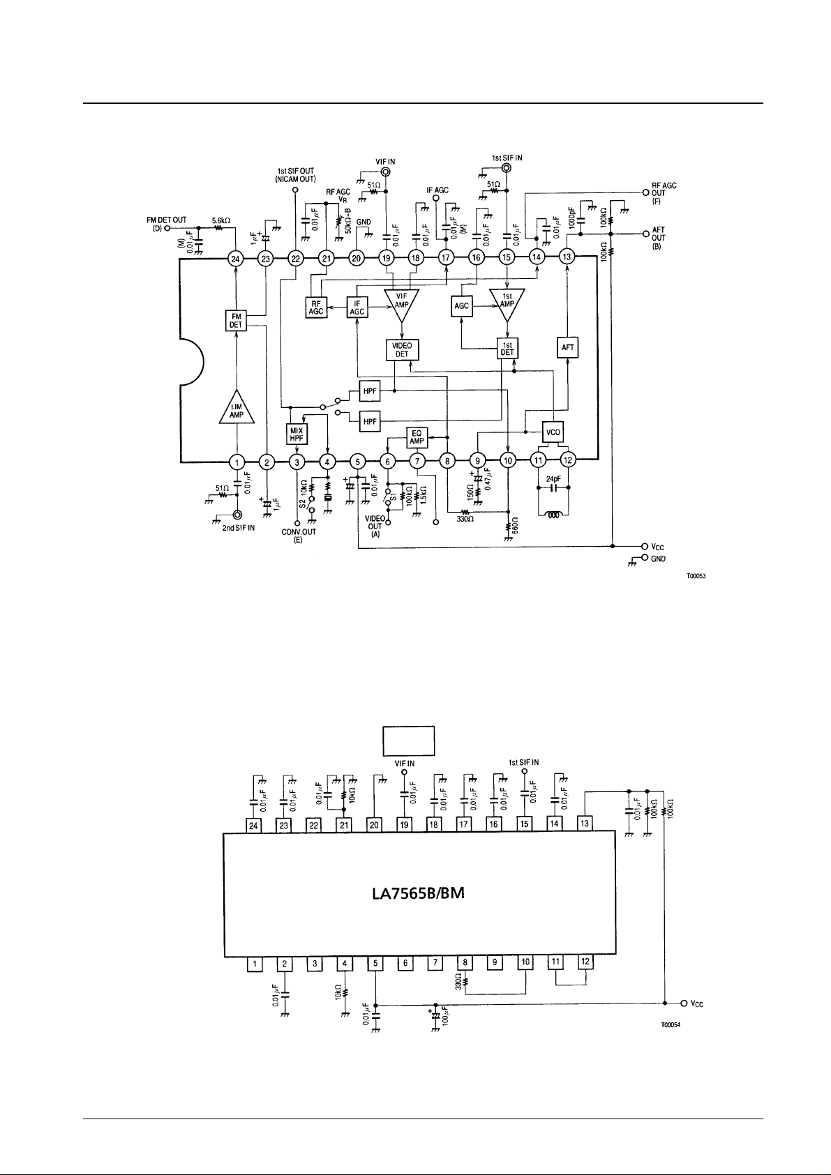
Internal Equivalent Circuit and External Circuit Diagram
No. 5636-4/16
LA7565B, 7565BM
68 Ω
AC Characteristics Test Circuit
Test Circuit
No. 5636-5/16
LA7565B, 7565BM
Impedance
analyzer
68 Ω
 Loading...