

Page 1
Any and all SANYO products described or contained herein do not have specifications that can handle
applications that require extremely high levels of reliability, such as life-support systems, aircraft’s
control systems, or other applications whose failure can be reasonably expected to result in serious
physical and/or material damage. Consult with your SANYO representative nearest you before using
any SANYO products described or contained herein in such applications.
SANYO assumes no responsibility for equipment failures that result from using products at values that
exceed, even momentarily, rated values (such as maximum ratings, operating condition ranges,or other
parameters) listed in products specifications of any and all SANYO products described or contained
herein.
Monolithic Linear IC
IF Signal Processing (VIF+SIF)
Circuit for TV / VCR Use
Ordering number:ENN2927
LA7555
SANYO Electric Co.,Ltd. Semiconductor Company
TOKYO OFFICE Tokyo Bldg., 1-10, 1 Chome, Ueno, T aito-ku, TOKYO, 110-8534 JAPAN
Overview
The LA7555 is a full sync detection method VIF + SIF
monolithic linear IC using a PLL. It has excellent 920kHz
beat and buzz beat characteristics, making it ideal for use
in audio multiplexing and high-quality AV equipment.
Functions
• VIF section
· VIF amplifier · Video sync detecton · IF AGC
· B/W NC · RG AGC · AFT
· VCO · APC DET · Lock DET
• SIF section
· SIF limiter amplifer · FM quadrature detection
• Audio section
· DC attenuator · AF driver
• Muting
· Audio muting (pin 2)
· AFT defeat (pin 14)
· Audio-Video simultaneous muting (pin 10, 13)
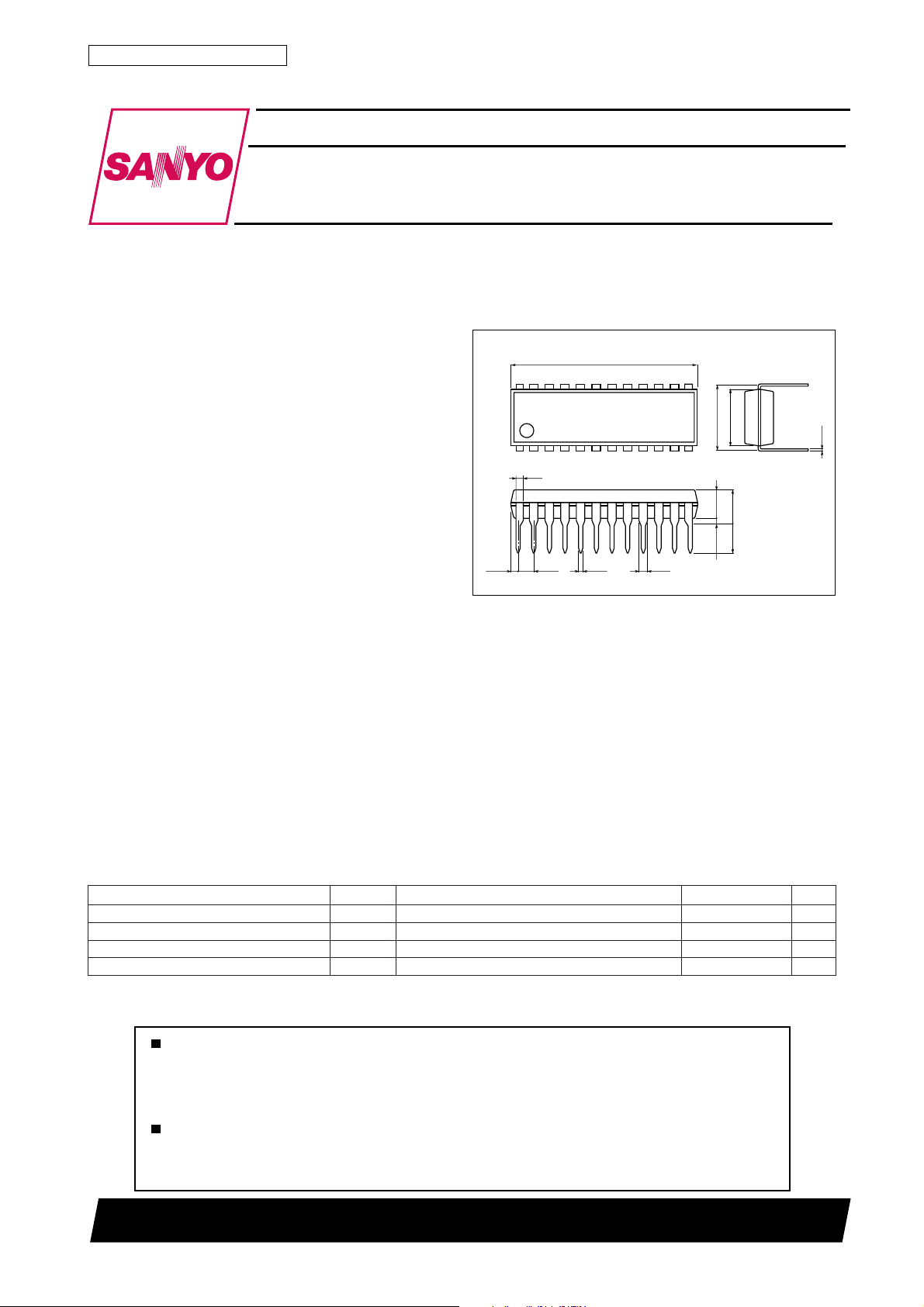
Package Dimensions
unit:mm
3067A-DIP24S
[LA7555]
21.0
(0.71)
24
1
0.9
1.78
0.48
0.95
13
7.62
12
(3.25)
0.51min
SANYO : DIP24S
6.4
0.25
3.9max
3.3
Features
• 24-pin DIP shrink package being the smallest one used
for PLL ICs.
• Excellent 920kHz beat characteristics.
• Excellent buzz beat characteristics.
• High-gain VIF amplifier.
• High-speed AGC possible.
• Excellent power supply ripple characteristics.
Specifications
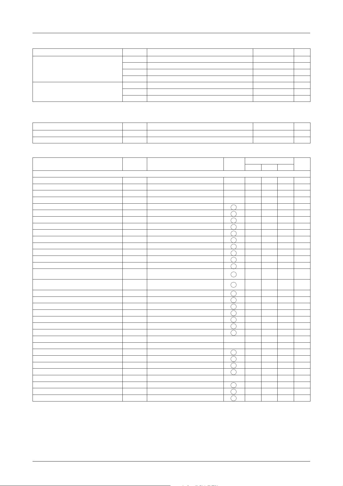
Maximum Ratings at Ta = 25˚C
retemaraPlobmySsnoitidnoCsgnitaRtinU
egatlovylppusmumixaMV
noitapissidrewopelbawollAxamdP 0021Wm
erutarepmetgnitarepOrpoT 07+ot02–
erutarepmetegarotSgtsT 051+ot55–
xam 8.31V
CC
Ta≤50˚C
O2500TN (KT)/N078YT, TS No.2927–1/11
˚C
˚C
Continued on next page.
Page 2
LA7555
Continued from preceding page.
retemaraPlobmySsnoitidnoCsgnitaRtinU
V21V,
31
V
egatlovtiucriC
tnerructiucriC
Note : Assumes that the current flowing into the IC is positive (no sign) and current flowing out of the IC is negative.
Operating Conditions at Ta = 25˚C
retemaraPlobmySsnoitidnoCsgnitaRtinU
egatlovylppusdednemmoceRV
egnaregatlovgnitarepOV
Operating Characteristics at Ta = 25˚C
retemaraPlobmySsnoitidnoC
]noitcesFIV[
tnerructiucriCI
egatlovtuptuooedivtnecseiuQV
egatlovCGAFRmumixaMV
egatlovCGAFRmuminiMV
egatlovtuptuoTFAtnecseiuQV
ytivitisnestupnIiVMA%04,zH004=mf339354Vµ/Bd
egnarCGARG0656Bd
tupnielbawollamumixaMxamiV001002smrVm
edutilpmatuptuooediV)oediv(oVMA%87,zHk51=mf9.12.25.2p-pV
N/StuptuON/SWC,Vm01=iV9435Bd
egatlovpitlangiscnySV
leveltaebzHk029I
citsiretcarahcycneuqerFf
egatlovlangistuptuoFIS)FIS(oVBd02–=S,0=P011081062smrVm
niaglaitnereffiDGD
esahplaitnereffiDPD
egatlovdlohserhtesionetihWV
egatlovpmalcesionetihWV
egatlovdlohserhtesionkcalBV
egatlovpmalcesionkcalBV
egatlovTFAmumixaMV
egatlovTFAmumimiMV
ytivitisnesnoitcetedTFAfS730507
ecnatsisertupnIirzHM57.85=f8.03.157.1kΩ
ecnaticapactupnIiczHM57.85=f0.30.6Fp
1)U(egnarni-llupCPAf
1)L(egnarni-llupCPAf
2)U(egnarni-llupCPAf
2)L(egnarni-llupCPAf
egatlovdlohserhtnoitcetedkcoLV
egnarelbairavmumixamOCV
egnarelbairavmumixamOCV
ytivitisneslortnocOCV
61
V
22
V
32
I
5
I
12
I
22
CC
po 2.31ot01V
CC
tseT
tnioP
6I+71
∆f
V31V11=71,6sniP547517Am
V31V11=12niP9.53.67.6V
12
V31V11=11niP6.01114.11V
H11
V31V11=11niP05.0V
L11
V31V11=5.35.65.7V
61
pitWC,Vm01=iV54.37.359.3V
12
029
c
HTW
LCW
HTB
LCB
H61
L61
1-UP
1-LP
2-UP
2-LP
HT31
V02V3=1.2zHM
U
∆f
V02V7=1.2–zHM
L
β
V
02
Bd41–=S,0=P67zHM
langisoediv
langisoediv
PEEWS,smrVm01=iV0.115.110.21V
PEEWS,smrVm01=iV05.00.1V
V6.4otV5=4.18.26.5
)p-pV2(Bd41–=S,Bd4–=C,0=P8364Bd
,%5.78dom,Vm01=iV,zHM57.85=pf
,%5.78dom,Vm01=iV,zHM57.85=pf
B
A
A
A
A
A
A
A
A
A
A
A
A
A
A
A
B
B
B
A
A
A
A
22niP115.11V
A
A
A
V
V
CC
V
V
CC
V
V
CC
V
V
CC
3–Am
5–Am
2Am
21V
sgnitaR
nimpytxam
38%
38ged
4.68.62.7V
2.46.40.5V
3.26.29.2V
1.45.49.4V
8.0zHM
8.0–zHM
2zHM
2–zHM
Continued on next page.
tinU
zHk/Vm
Vm/zHk
No.2927–2/11
Page 3
LA7555
Continued from preceding page.
retemaraPlobmySsnoitidnoC
]noitcesFIS[
egatlovgnitimilFIS)mil(iVV31V5=061023smrVµ
egatlovtuptuonoitcetedMFoVV31V5=3.5–8.1–4.0+*sBd
noitcejerMARMAV31V5=0455Bd
noitrotsiD)teD(DHTV31V5=5.01%
]noitcesoiduA[
noitaunettamumixamRVCDA
niagegatlovreifilpmaFAG
noitrotsidreifilpmaFA)FA(DHTV32V,V8=
egatlovtuptuomumixamreifilpmaFA
TT
FA
V32V8= → V,V0
)FA(xamoV
V
32
V5=0757Bd
31
V,V8=32V
V5=810222Bd
31
31
V,V8=
V5=34smrV
31
zH004=f,V5=5.01%
tseT
tnioP
nimpytxam
C
C
C
C
D
D
D
D
* : 0dBs=0.7745Vrms
A : Video output (pin21), B : AFT output (pin16), C : FM detection output (pin1), A : Audio output (pin5)
sgnitaR
tinU
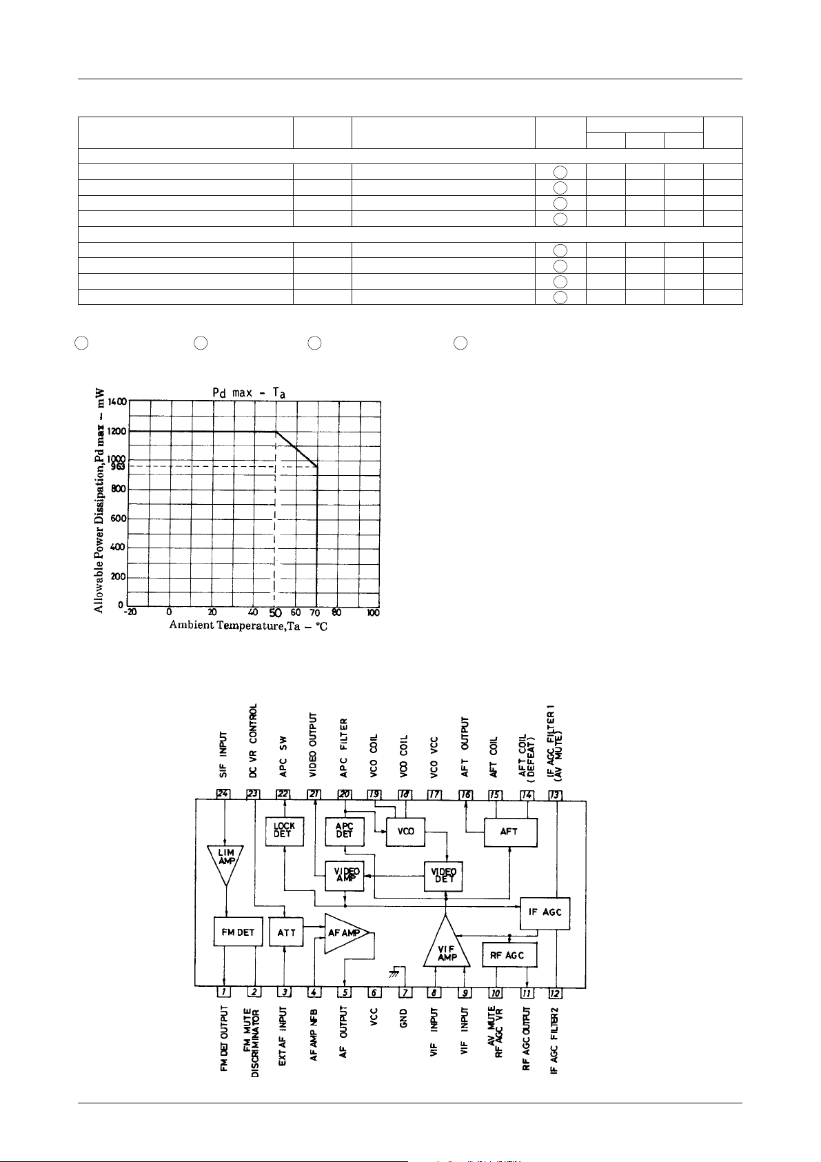
Equivalent Circuit Block Diagram
No.2927–3/11
Page 4
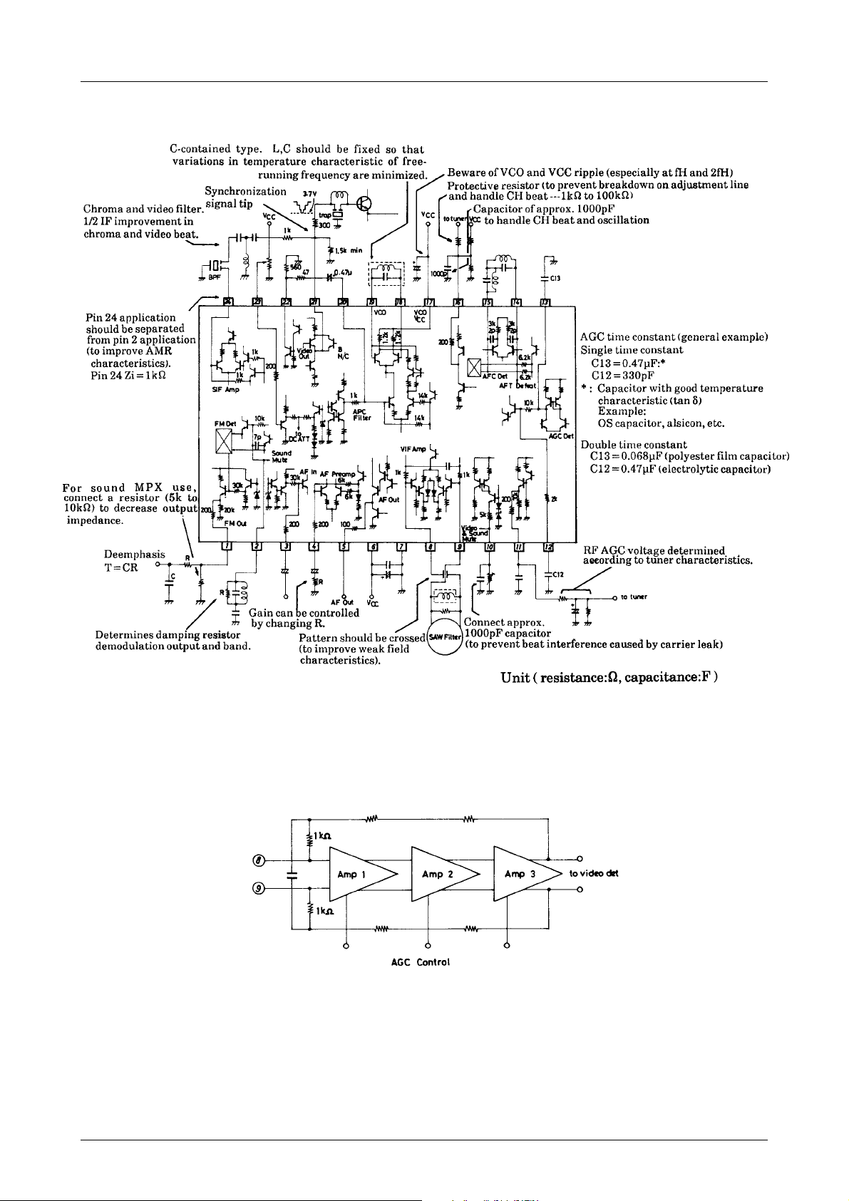
Precautions when using the LA7555
LA7555
Description of Operation
1. IF amplifier
As shown in Fig.1-1, the IF amplifier consists of three amplifiers directly connected with balanced input.
Amplifiers 1, 2 and 3, and the gain are controlled by the AGC.
Fig.1-1
No.2927–4/11
Page 5

LA7555
2. Video detector
As shown in Fig.2-1, the video detector is a PLL-type. AM detection (video detection) is by phase shifting the IF
signal and VCO output signal 180° and multiplying the input signal. It offers excellent buzz and beat characteristics as detection is by multiplication by a clean signal. Also, excellent detection characteristics are obtained in the
same manner for the overmodulation signal.
Fig.2-1
3. Video amplifier B/W noise canceller
As shown in Fig.3-1, the video amplifier amplifies the detection output voltage over a wide band to the desired
voltage (=2.2Vp-p). The amplified video signal passes through the B/W noise canceller and is output to pin 21.
White : The noise canceller operates as shown in Fig.3-3 as the input of noise exceeding the white level of the
video signal as shown in Fig.3-2 will cause noticeable noise on the screen.
Black : The noise canceller operates as shown in Fig.3-3 as the input of noise exceeding the sync signal tip as
shown in Fig.3-2 will prevent proper operation of the next-stage sync separation circuit.
Fig.3-1
Fig.3-2 Fig.3-3
No.2927–5/11
Page 6

LA7555
4. Lock detector
As shown in Fig.4-1, the lock detector is an APC time constant switching detection circuit which expands the APC
pull-in range. The detection circuit operates by the OR of the IF AGC voltage and the video signal. The weak field
is detected by the IF AGC voltage and the unlock state when detuned is detected from the video signal.
Fig.4-1
5. AGC detector
As shown in Fig.5-1, the AGC detector is equipped with a noise canceller function which prevents malfunction of
the AGC system. The AGC detection output (pin 13) is also used for video output, FM detection output, and as the
simultaneous mute (AV MUTE) pin.
Fig.5-1
6. RF AGC
As shown in Fig.6-1, the RF AGC controls the gain of the tuner’s RF amplifier. Measurement is made whether the
region is snow region (noise on the screen, poor S/N ratio) or a saturation region (contours can be clearly seen but
look bad due to video signal distortion), and the RF AGC delay point is set as shown in Fig6-2. Pin 10 is also used
for video output, FM detection output, and as the simultaneous mute (AV MUTE) pin.
Fig.6-1
Fig.6-2
No.2927–6/11
Page 7

LA7555
7. AFT
As shown in Fig.7-1, the AFT is a balanced-type using a quadrature detection circuit. The input signal is shifted
90° by the internal capacitor and external phase shifter, and quadrature-detected. Pin 14 is also used as the AFT
Defeat pin. Fig.7-1
Fig.7-1
C2 forms a sound trap for preventing malfunction of the AFT.
8. SIF limiting amplifier
As shown in Fig.8-1, the SIF limiting amplifier is an unbalanced limiting amplifier consisting of four stages
derectly connected. There is negative feedback within the IC to balance the differential amplifier.
Fig.8-1
9. Quadrature detection
SIF quadrature detection is by the single pin detector with internal phase shift capacitor, shown in Fig.9-1. FM
detection is by shifting the SIF signal 90° and multiplying it. The characteristics of the phase shifting circuit are as
follows :
1. Demodulation output .....mainly Q
L
2. Distortion ... linearity of phase shifting circuit, symmetry of S curve.
The linearity of the phase shifting circuit can be improved by lowering QL and increasing the band with a singletuned circuit, but the FM detection output will drop.
Pin 2 is also used as the SIF mute pin.
Fig.9-1
10.Electronic volume control
As shown in Fig.10-1, this is an electronic volume control, having a control pin with high input impedance. The
attenuation curve is a logarithmic curve. The external audio input impedance is approximately 30kΩ.
No.2927–7/11
Page 8

LA7555
Fig.10-1
11.AF amplifier
As shown in Fig.11-1, this is an AF amplifier equipped with an NFB pin. An audio power amplifier can be easily
configured by use of this NFB pin. The gain of the power amplifier can be controlled by the ratio of R1 and R2.
Fig.11-1
VCO adjustment methods
The following two methods are available for adjusting the VCO.
1. APC voltage offset adjustment method
a. Connect a digital voltmeter to pin 20 (APC filter pin ) (Fig.1).
b. Lower the IF input level and connect the IF AGC (pin 13) to GND.
Measure the voltage on pin 20 at this time.
c. Raise the IF input level to the desired value. Free the IF AGC from GND (internal AGC). Adjust the VCO so
that the voltage (V2) on pin 20 is equal to V1.
Note : When adjusting by this method, use a DVM (digital voltme-
ter) with high input impedance. At Zi=10MΩ, the adjustment
error is approximately 20kHz, The error (∆V) with the DVM
connected is.
Fig.1
R
∆V (mV)= V (1– )
Z+R
1
1
The change in VCO free-running frequency (∆f) according to
∆V is ∆f (kHz)=∆V× β
where β=VCO control sensitivity (kHz/mV)
2. Direct reading method
a. Lower the IF input level and adjust the IF AGC (pin 13) to between GND and about 4V (VCO free run).
b. Monitor the carrier frequency leaking from pins other than the VCO coil, or pattern, chassis, and adjust the
VCO coil to obtain the desired frequency (fp).
No.2927–8/11
Page 9

LA7555
Measurement of VIF selectivity characteristics
The pull-in range of the PLL-type VIF IC is approximately ±2MHz. Thus, it is not possible to measure the matching characteristics of the tuner SAW filter easily as with the dummy syncronization detection method. The following is just one example of how to measure the selectivity characteristics for a single signal.
Test Circuit
Conditions
1. Apply voltage to the IF AGC (pin 13) and adjust until the video output A is 0.5Vp-p.
2. Atteach a 4.7µF capacitor to the APC filter (pin 20) so that the PLL is unlocked.
3. The waveform shown in the diagr am below can be monitored through the externally mounted detector.
Note : Error will occur in the measurement of the selectivity characteristics if the video frequency changes between
A and C (by a video equalizer, etc.)
Externally Mounted Detector (Example)
(1) (2) Voltage doubler type
No.2927–9/11
Page 10

Sample Application Circuit (JAPAN)
LA7555
Item
JAPAN
fP=58.75MHz
US
fP=45.75MHz
PAL
fP=38.9MHz
T1 : VCO coil T2 : AFT coil T3 : SIF coil
7mm square
0.12φ 6t
C=24pF PH
S-CORE
HW-6226-4
MITSUMI
7mm square
0.12φ 9t
C=24pF PH
S-CORE
HW-6227-4
MITSUMI
7mm square
0.12φ 11t
C=24pF PH
S-CORE
MA-6389
MITSUMI
7mm square
0.5φ 3 1/2t
External c=91pF
MA-6342
MITSUMI
7mm square
0.5φ 5 1/2t
External c=91pF
MA-6343
MITSUMI
7mm square
0.5φ 6 1/2t
External c=91pF
MA-7115
MITSUMI
7mm square
0.08φ
19t - 19t
C=100pF
KS-6102-1
MITSUMI
7mm square
0.08φ
19t - 19t
C=100pF
KS-6102-1
MITSUMI
SW filter
SAW Filter
TSF1110 SANYO
SAW Filter
TSF1203 SANYO
TSF1212 SANYO
SAW Filter
TSF1303 SANYO
No.2927–10/11
Page 11

LA7555
Specifications of any and all SANYO products described or contained herein stipulate the performance,
characteristics, and functions of the described products in the independent state, and are not guarantees
of the performance, characteristics, and functions of the described products as mounted in the customer's
products or equipment. To verify symptoms and states that cannot be evaluated in an independent device,
the customer should always evaluate and test devices mounted in the customer's products or equipment.
SANYO Electric Co., Ltd. strives to supply high-quality high-reliability products. However, any and all
semiconductor products fail with some probability. It is possible that these probabilistic failures could
give rise to accidents or events that could endanger human lives, that could give rise to smoke or fire,
or that could cause damage to other property. When designing equipment, adopt safety measures so
that these kinds of accidents or events cannot occur. Such measures include but are not limited to protective
circuits and error prevention circuits for safe design, redundant design, and structural design.
In the event that any or all SANYO products(including technical data,services) described or
contained herein are controlled under any of applicable local export control laws and regulations,
such products must not be exported without obtaining the export license from the authorities
concerned in accordance with the above law.
No part of this publication may be reproduced or transmitted in any form or by any means, electronic or
mechanical, including photocopying and recording, or any information storage or retrieval system,
or otherwise, without the prior written permission of SANYO Electric Co. , Ltd.
Any and all information described or contained herein are subject to change without notice due to
product/technology improvement, etc. When designing equipment, refer to the "Delivery Specification"
for the SANYO product that you intend to use.
Information (including circuit diagrams and circuit parameters) herein is for example only ; it is not
guaranteed for volume production. SANYO believes information herein is accurate and reliable, but
no guarantees are made or implied regarding its use or any infringements of intellectual property rights
or other rights of third parties.
This catalog provides information as of October, 2000. Specifications and information herein are subject
to change without notice.
PS No.2927–11/11
 Loading...