

Page 1
Ordering number : ENN*6930
41301RM (OT) No. 6930-1/13
Overview
The LA75505M is a VIF/SIF signal processing IC for
NTSC TV/VCR. It supports the 45.75 MHz and 58.75
MHz as the IF frequencies. On-chip sound carrier trap and
sound carrier BPF circuits make it ideal for compact and
light-weight tuner applications. To adjust the VCO circuit,
AFT circuit, and sound filter, 4-MHz external crystal or 4MHz external signal is needed.
Functions
• VIF amplifier
• VCO adjustment free PLL detection circuit
• Digital AFT circuit
• RF AGC
• Buzz canceller
• Equalizer amplifier
• Internal sound carrier BPF
• Internal sound carrier trap
• PLL-FM detector
• Reference oscillation circuit
Features
• Internal VCO adjustment free circuit eliminating need
for VCO coil adjustments.
• Considerably reduces the number of required peripheral
parts by providing on-chip sound carrier BPF and sound
carrier trap circuits.
•Use of digital AFT eliminates problem of AFT
tolerance.
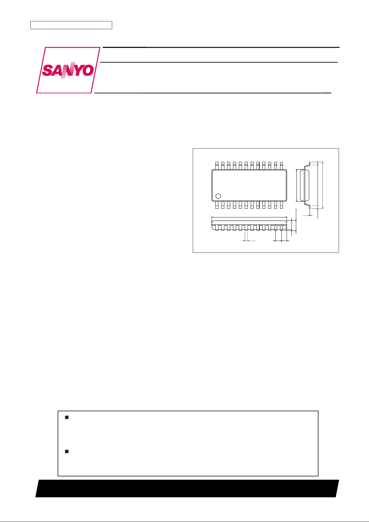
• Package: MFP24S (300 mil)
Package Dimensions
unit: mm
3112-MFP24S
112
24
13
12.6
0.8
1.0
0.15
0.35
5.4
6.35
7.6
0.625
1.8max
1.5
0.1
Preliminary
SANYO: MFP24S (300 mil)
[LA75505M]
LA75505M
SANYO Electric Co.,Ltd. Semiconductor Company
TOKYO OFFICE Tokyo Bldg., 1-10, 1 Chome, Ueno, Taito-ku, TOKYO, 110-8534 JAPAN
Adjustment Free VIF/SIF Signal Processing IC
for TV/VCR
Monolithic Linear IC
Any and all SANYO products described or contained herein do not have specifications that can handle
applications that require extremely high levels of reliability, such as life-support systems, aircraft’s
control systems, or other applications whose failure can be reasonably expected to result in serious
physical and/or material damage. Consult with your SANYO representative nearest you before using
any SANYO products described or contained herein in such applications.
SANYO assumes no responsibility for equipment failures that result from using products at values that
exceed, even momentarily, rated values (such as maximum ratings, operating condition ranges, or other
parameters) listed in products specifications of any and all SANYO products described or contained
herein.
Page 2
No. 6930-2/13
LA75505M
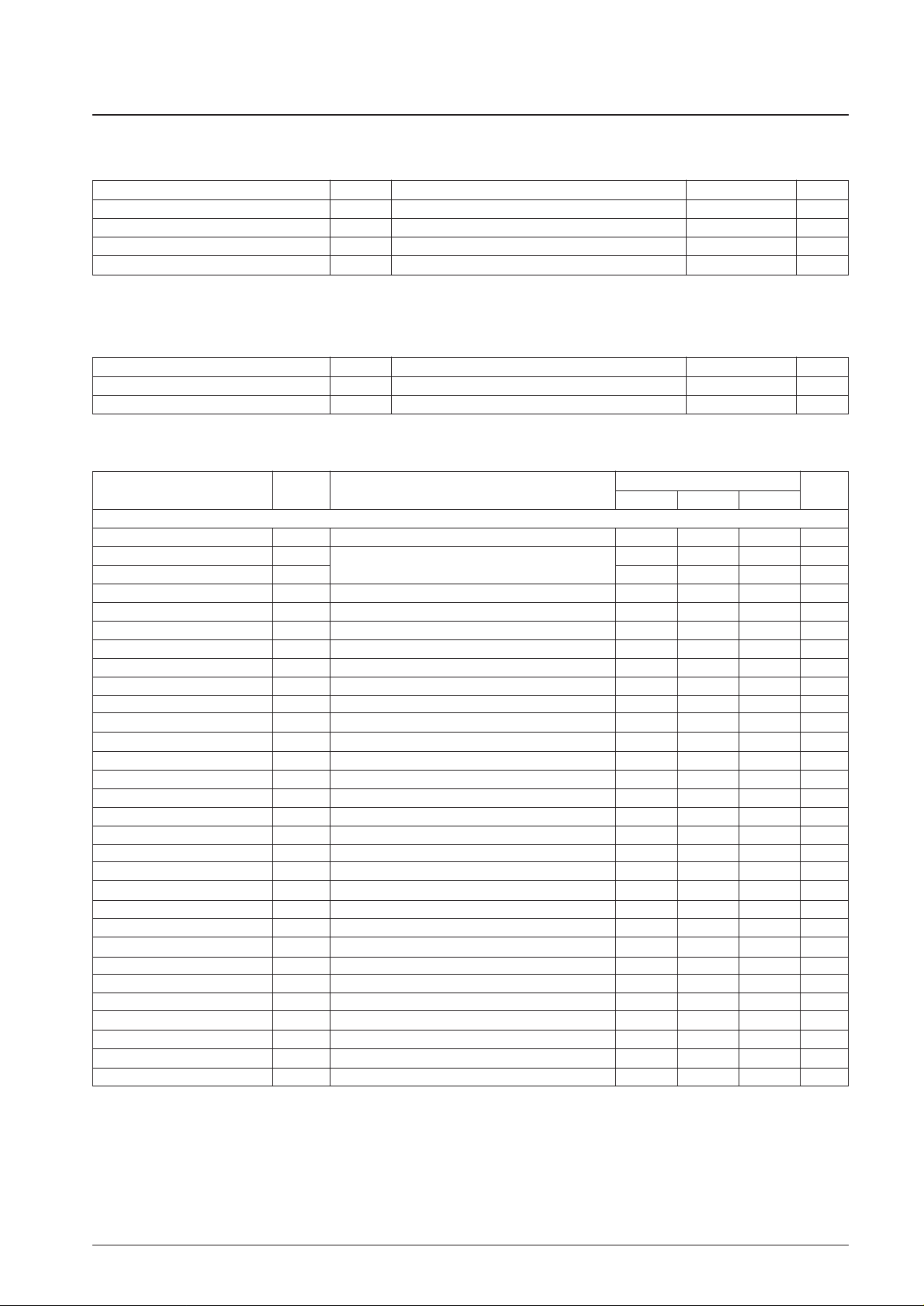
Parameter Symbol Conditions Ratings Unit
Maximum supply voltage V
CC
max 7 V
Allowable power dissipation Pd max Ta ≤ 70°C (*Mounted on a printed circuit board) 470 mW
Operating temperature Topr –20 to +70 °C
Storage temperature Tstg –55 to +150 °C
Specifications
Maximum Ratings at Ta = 25°C
Parameter Symbol Conditions Ratings Unit
Recommended supply voltage V
CC
5 V
Operating voltage range V
CC
op 4.5 to 5.5 V
Operating Conditions at Ta = 25°C
Parameter Symbol Conditions
Ratings
Unit
min typ max
[VIF Block ]
Circuit current I17 64.0 73.6 mA
Maximum RF AGC voltage V14H Collector load 30 kΩ VC2 = 9 V 8.5 9 — V
Minimum RF AGC voltage V14L 0.3 0.7 V
Input sensitivity Vi 33 39 45 dBµV
AGC range GR 58 dB
Maximum allowable input Vimax 92 97 dBµV
No-signal video output voltage V4 3.3 3.6 3.9 V
Synchronizing signal tip voltage V4tip 1.0 1.3 1.6 V
Video output level V
O
1.7 2.0 2.3 Vpp
Video signal-to-noise ratio S/N 46 50 dB
C-S beating IC-S P/S = 10 dB 26 32 38 dB
Differential gain DG Vin = 80 dBµ 3 10 %
Differential phase DP 2 10 deg
VIF input resistance Ri 2.5 3.0 kΩ
VIF input capacitance Ci 3 6 PF
Maximum AFT voltage V13H 4.3 4.7 5.0 V
Minimum AFT voltage V13L 0 0.2 0.7 V
AFT tolerance 1 dfa1 f = 45.75 MHz ±35 ±45 kHz
AFT tolerance 2 dfa2 f = 58.75 MHz ±45 ±70 kHz
AFT detection sensitivity Sf RL = 100 kΩ//100 kΩ 40 80 120 mV/kHz
AFT dead zone fda 60 100 kHz
APC pull-in range (U) fpu 1.0 1.5 MHz
APC pull-in range (L) fpl 1.0 1.5 MHz
VCO maximum frequency range (U)
dfu 1.5 2.0 MHz
VCO maximum frequency range (L)
dfl 1.5 2.0 MHz
VCO control sensitivity
β 2.0 4.0 8.0 kHz/mV
N trap1 (4.75 MHz) NT1 wrt 1 MHz –30 –35 dB
N trap2 (5.25 MHz) NT2 wrt 1 MHz –19 –24 dB
Group delay 1 NTSC (3.0 MHz) NGD1 wrt 1 MHz 10 40 70 ns
Group delay 1-1 NTSC (3.5 MHz) NGD1-1 wrt 1 MHz 70 120 170 ns
Electrical Characteristics at Ta = 25°C, VCC= 5.0 V, fp = 45.75 MHz
Note: * Circuit board dimensions: 114.3 × 76.1 × 1.6 mm3, material: glass epoxy
Continued on next page.
Page 3
No. 6930-3/13
LA75505M
Continued from preceding page.
Parameter Symbol Conditions
Ratings
Unit
min typ max
[1st SIF Block]
Conversion gain Vg fp = 4.5 MHz, Vi = 500µV 26 32 dB
SIF carrier output level So Vi = 10 mV 100 mVrms
First SIF maximum input Simax So ±2 dB 106 dBµV
First SIF input resistance Ris 5.0 6.0 kΩ
First SIF input capacitance Cis 3 6 pF
[SIF Block]
Limiting sensitivity Vi(lim)
fp = 4.5 MHz, ∆F = ±25 kHz at 400 Hz
61 dBµV
FM detector output voltage Vo(FM) 480 600 750 mVrms
AM rejection ratio AMR AM = 30% at 400 Hz 50 60 dB
Total harmonic distortion THD f = 4.5 MHz, ∆F = ±25 kHz 0.5 1.0 %
FM detector output S/N
S/N(FM) 55 60 dB
BPF 3-dB bandwidth
BW ±100 kHz
NTSC de-emphasis
Ndeem fm = 2 kHz –3 dB
[Others]
4-MHz level (during external input)
X4MIN Terminated 86 dBµ
IF system SW threshold resistance
V12 270 kΩ
Split/inter SW V16 0.5 V
Page 4
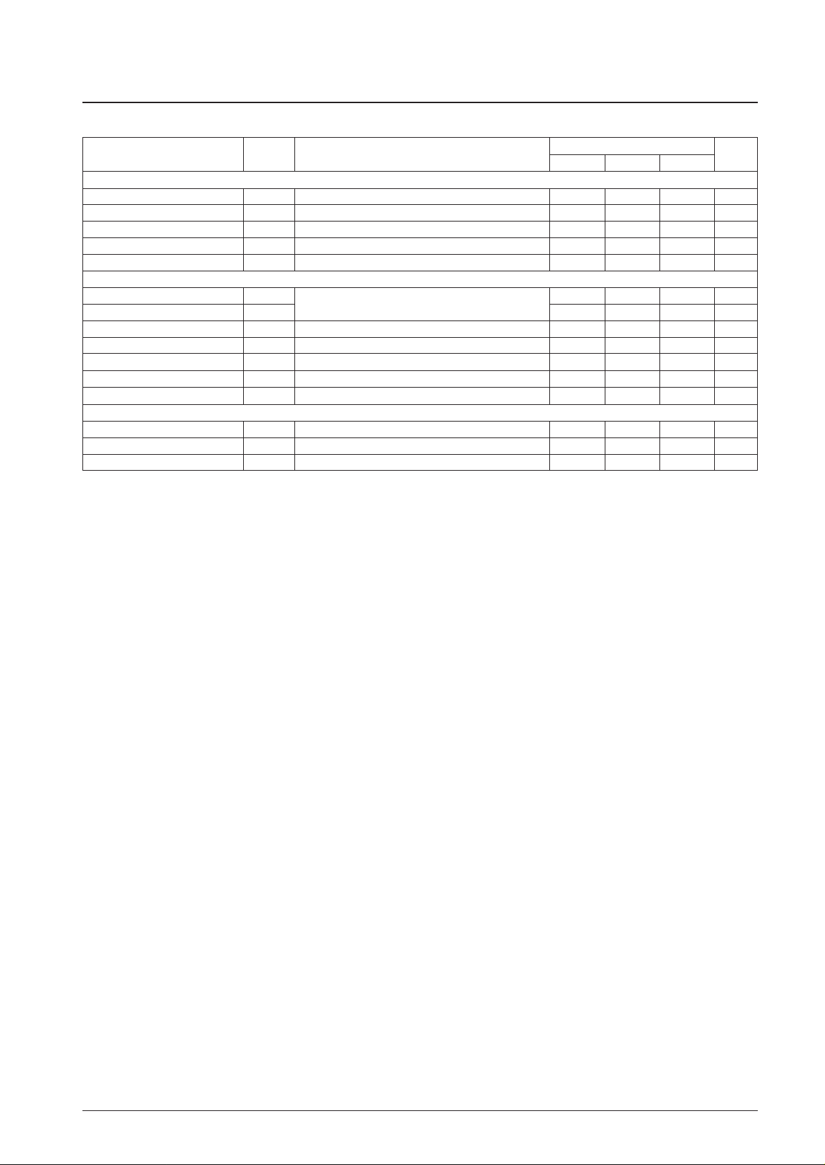
System Switching
No. 6930-4/13
LA75505M
• IF system switch
45.75 MHz is selected as the IF frequency by leaving pin 12 (crystal oscillation) open. 58.75 MHz is selected by
adding 220 kΩ between pin 12 and GND.
• Split/inter carrier switch
Inter carrier is selected by setting the first SIF input (pin 16) to GND.
Pin Assignment
19
2
1
SIF INPUT
FM FILTER
1st SIF OUT
VIDEO DET OUT
EQ OUT
APC FILTER
FLL FILTER
VCO COIL
VCO COIL
SIF AGC FILTER
NC
REF OSC
FM DET OUT
RF AGC VR
SIF PLL FILTER
FILTER CONTROL CAPACITOR
VIF INPUT
VIF INPUT
GND
VCC
1st SIF INPUT
IF AGC FILTER
RF AGC OUT
AFT OUT
3
4
5
6
7
8
9
16
17
18
20
21
22
23
24
10
11
12
13
14
15
Top view
LA75505M
Page 5

No. 6930-5/13
LA75505M
Test Circuit
Input Impedance Measuring Circuit (VIF, First SIF input impedance)
24 23 22 21 20 19 18 17 16 15 14 13
1 2 3 4 5 6 7 8
9
10 11 12
0.01 µF
0.01 µF
0.01 µF
0.01 µF
0.01 µF
0.01 µF
0.01 µF
0.01 µF
0.01 µF
0.01 µF
0.01 µF
0.01 µF
100 µF
10 kΩ
1 kΩ
15 kΩ
0.01 µF
0.01 µF
VIF INPUT
Impedance analyzer
1st SIF INPUT
VCC
LA75505M
Top view
+
0.01 µF
0.01 µF
0.01 µF
0.01 µF
0.01 µF
0.01 µF
Page 6

No. 6930-6/13
LA75505M
Pin Functions
Pin No. Pin Pin Function Internal Circuit
Inputs the SIF signal from the first SIF output.
Set the input level to 90 dBµV or lower because of
the dynamic range of the internal filter.
1 SIF INPUT
This is the FM feedback filter pin. It is composed of
a C and R filters.
1 µF is normally used as the capacitance.
If the capacitance is a low value, the audio output
level is small at low frequencies.
Moreover, the audio output level can be made
smaller by increasing the resistance connected in
series.
Use a resistance of 3 kΩ or higher.
2 FM FILTER
This is the first SIF output.
In case of inter carrier, the chroma carrier is bigger
than split carrier applications, so that it is
recommended to connect a filter externally.
3
1st SIF OUT
Filter example
Continued on next page.
Page 7

No. 6930-7/13
LA75505M
Continued from preceding page.
Continued on next page.
Pin No. Pin Pin Function Internal Circuit
Pin 4 is the video output pin.
The EQ amplifier can be thought of as shown
below.
4
5
VIDEO-OUT
EQ-OUT
output
Time
constant switch
output
Pin 6 is the PLL detector APC filter pin.
Normally the following are used:
R = 330 Ω
C1 = 0.47 µ to 1 µF
C2 = 100 pF
C1 = 1 µF is effective for the overmodulation
characteristics.
When the PLL is locked, the signal passes via the
path marked A in the figure, and when PLL is
unlocked and in weak signal, the signal passes via
the path marked B in the figure. The PLL loop gain
can thus be switched in this manner.
Pin 7 is a VCO automatic control FLL filter pin.
Since it operates always on a small current, using a
larger capacitance results in a slower response.
Normally, a capacitance between 0.47 µF and 1 µF
is used.
Moreover, the control range for this pin is between
about 3 V to 4.7 V. Since this range is determined
when adjusting the VCO tank circuit, set the design
center of L and C of VCO so that the voltage of pin
7 is 3.6 V.
6
7
APC FILTER
FLL FILTER
Therefore, the peak gain of the EQ amplifier is
determined by Av = 1 + R/Z.
However, note that the LA75505M being an IC with
V
CC
= 5 V, setting too large an amplitude causes
distortion in the V
CC
side. Use so that the white
level is 4 V or less.
This is the VCO tank circuit for the PLL detector.
Use a tuning capacitance of 24 pF.
For the L and C specifications, use IF45.75 MHz
specifications within ±1.5%, and 58.75 MHz
specifications within ±1%. Also, design the L and C
values so that the voltage of pin 7 is 3.6 V when
PLL is locked while using the IF center frequency.
8
9
VCO COIL
Page 8

No. 6930-8/13
LA75505M
Continued from preceding page.
Pin No. Pin Pin Function Internal Circuit
This pin can be used both as the crystal resonator
pin and IF switch.
The 58.75-MHz mode is selected by inserting 220
kΩ between pin 12 and GND, the 45.75 MHz mode
by leaving the pin open.
4-MHz input is possible from this pin.
In the case of 4-MHz external input, input 86 dBµ
or more.
12
REF OSC
Continued on next page.
Pin 10 is the SIF AGC filter pin. Use a capacitance
of 0.01 µF to 0.1 µF.
10
SIF AGC FILTER
10
Not connected
11
NC
Pin 13 is the AFT output pin.
Use external resistors of 47 kΩ and a filter
capacitance 0.1 µF.
The AFT circuit generates the AFT voltage by
comparing the signal obtained by dividing the
4-MHz reference frequency with the signal obtained
by dividing VCO.
Since it uses a digital phase comparator, a dead
zone exists in the AFT center.
13
AFT OUT
waveform
Page 9

No. 6930-9/13
LA75505M
Continued from preceding page.
Pin No. Pin Pin Function Internal Circuit
Pin 14 is the RF AGC output.
RF AGC max is determined by R1 and R2.
RF AGC min is determined by R3 and R4.
Capacitor C1 prevents oscillation and capacitor C2
is the RF AGC filter.
Normally 30 kΩ is used for R1, but if the tuner's F/E
transistor is GaAS, the gate's impedance is lower,
so use approx. 10 kΩ.
14
RF AGC OUT
Pin 15 is the IF AGC filter pin.
Normally, 0.01 µF to 0.02 µF polyester film
capacitor is used.
Determine the impedance based on H-SAG and
AGC speed.
15
IF AGC FILTER
Continued on next page.
Pin 16 can be used both as the First SIF IN and
inter/split switch pins.
In the case of inter carrier, connect pin 16 to GND.
When a sound saw filter is added, the matching
loss can be decreased by inserting L to neutralize
the IC input capacitance and saw filter output
capacitance.
16 1st SIF INPUT
Page 10

No. 6930-10/13
LA75505M
Continued from preceding page.
Pin No. Pin Pin Function Internal Circuit
Pins 19 and 20 are VIF input pins.
To reduce the loss of signal through a saw filter,
input registors are set to 2 kΩ.
VIF amplifier has three capacitive coupling
amplifiers, direct connection from a saw filter is
available.
19
20
VIF INPUT
Continued on next page.
Connect the decoupling capacitor as close as
possible.
17
V
CC
18
GND
Internal filters (i.e. sound carrier BPF and sound
carrier trap) are tuned using the capacitor
connected to pin 21.
A value between 0.47 µF and 1 µF is considered
desirable taking video S/N, and AM and PM noise
into consideration.
21
FILTER CONTROL
CAPACITOR
Page 11

No. 6930-11/13
LA75505M
Continued from preceding page.
Pin No. Pin Pin Function Internal Circuit
22
SIF PLL FILTER
Pin 22 is the SIF PLL filter pin.
Normally use the following values.
R: 3 kΩ
C1: 0.01 µF
C2: 1000 pF
When R is too large, the PLL may become
unlocked, so use a resistance value within 6 kΩ. A
smaller R value results in low-pass noise.
Pin 23 is the RF AGC VR pin.
When this pin is connected to GND, no signal is
appeared on pin 4 and pin 24.
23
RF AGC VR
24
FM DET OUT
Pin 24 is the FM output pin.
Time constance of de-emphasis is determined by
external C, R.
Please chose C, R to make time constance 75 µs.
Page 12

No. 6930-12/13
LA75505M
Sample Application Circuit
FM
DET
LIM
AMP
BPF
BPF
FM
DET
IF
AGC
VIF
AMP
1st
AMP
AGC
AFT
AMP
S
PLL
FLL
VCO LPF
TRAP
EQ
AMP
FIL
CONT
AMP
SW
VIDEO
DET
APC
DET
1stSIF
DET
1µ
3k
39p
CARRIER OUT
2k
VIDEO OUT
330
1µ
VCO COIL
1µ
4MHz
X’tal
220k
IF SW
OPEN:45.75MHz
GND :58.75MHz
0.01µ
7.5k
AUDIO
OUT
1000p
0.01µ
3k
1µ
0.1µ
AFT OUT
47k
47k
Unit
Capacitance: F
Resistance: Ω
RF
AGC OUT
0.02µ
0.01µ
0.01µ
100µ
30k
0.01µ
IF INPUT
VCC(5V)
VCC(9V)
SAW(P)
SAW(S)
0.01µ
24 23 22 21 20 19 18 17 16 15 14 13
121110
987654321
Page 13

PS No. 6930-13/13
LA75505M
This catalog provides information as of April, 2001. Specifications and information herein are subject to
change without notice.
Specifications of any and all SANYO products described or contained herein stipulate the performance,
characteristics, and functions of the described products in the independent state, and are not guarantees
of the performance, characteristics, and functions of the described products as mounted in the customer’s
products or equipment. To verify symptoms and states that cannot be evaluated in an independent device,
the customer should always evaluate and test devices mounted in the customer’s products or equipment.
SANYO Electric Co., Ltd. strives to supply high-quality high-reliability products. However, any and all
semiconductor products fail with some probability. It is possible that these probabilistic failures could
give rise to accidents or events that could endanger human lives, that could give rise to smoke or fire,
or that could cause damage to other property. When designing equipment, adopt safety measures so
that these kinds of accidents or events cannot occur. Such measures include but are not limited to protective
circuits and error prevention circuits for safe design, redundant design, and structural design.
In the event that any or all SANYO products (including technical data, services) described or contained
herein are controlled under any of applicable local export control laws and regulations, such products must
not be exported without obtaining the export license from the authorities concerned in accordance with the
above law.
No part of this publication may be reproduced or transmitted in any form or by any means, electronic or
mechanical, including photocopying and recording, or any information storage or retrieval system,
or otherwise, without the prior written permission of SANYO Electric Co., Ltd.
Any and all information described or contained herein are subject to change without notice due to
product/technology improvement, etc. When designing equipment, refer to the “Delivery Specification”
for the SANYO product that you intend to use.
Information (including circuit diagrams and circuit parameters) herein is for example only; it is not
guaranteed for volume production. SANYO believes information herein is accurate and reliable, but
no guarantees are made or implied regarding its use or any infringements of intellectual property rights
or other rights of third parties.
 Loading...