

Page 1
Monolithic Linear IC
Ordering number : EN5110
51595TH (OT) No. 5110-1/7
SANYO Electric Co.,Ltd. Semiconductor Bussiness Headquarters
TOKYO OFFICE Tokyo Bldg., 1-10, 1 Chome, Ueno, Taito-ku, TOKYO, 110-8534 JAPAN
NTSC Format Single-Chip Signal Processing IC
for VHS VCR Products
LA7425
Overview
The LA7425 is a single-chip video signal processing IC
for use in VHS format VCR products. The number of
required adjustments has been reduced to a single
adjustment by IC chip internal trimming. The
incorporation of a playback equalizer and other circuits on
chip provides a significant reduction in external
components and thus significantly reduces the cost of
manufacturing the signal processing printed circuit board.
This product can also support simplified S-VHS playback,
which is becoming a standard feature in VCR products in
the Japanese market.
Features
• Only one adjustment point (comb filter phase
adjustment)
(The AGC, carrier, deviation and PB-Y level are
adjustment free.)
(If an LA7411/16 is used as the head amplifier, the Y/C
record current will also be adjustment free.)
• Simplified S-VHS playback support
— Built-in S-VHS discrimination circuit
— Built-in equalizer switch
— Automatic demodulator gain switching
— Internal automatic de-emphasis characteristics
switching
• Only a minimal number of external components
required (85 components: This corresponds to a 38%
reduction over previous Sanyo products ... CNR and
SQPB not handled, and REC EQ not included.)
Components newly incorporated on chip:
— Playback equalizer (include chroma trap), limiter
balance filter, capacitor and resistor for detail
enhancer, record chroma 7.8 MHz trap, playback
chroma LPF, ACC filter
• High performance/multifunctionality
Linear phase type picture controller
Double high-pass noise canceller, high-speed AFC,
DCC
New built-in functions
— FM AGC, synchronization detection circuit, linear
control circuit for high-pass noise canceller,
playback mode Y/C separator output, chroma noise
canceller
• Single CCD system
The LA7425 supports the following functions with the
addition of only a single CCD (1H delay) device: comb
filter, YNR, DOC and chroma crosstalk cancellation.
Thus the cost of external components is lowered.
• Full HQ support (YNR, CNR, detail enhancer and WCL
up)
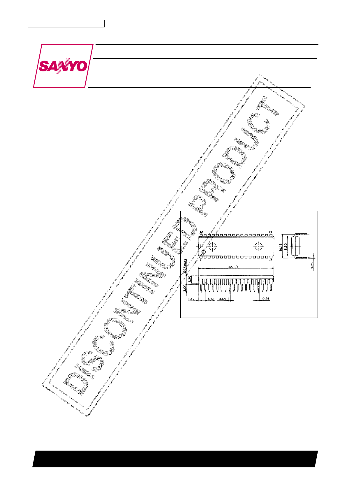
Package Dimensions
unit: mm
3170-DIP36S
SANYO: DIP36S
[LA7425]
Page 2
Functions
All VHS format VCR (NTSC) signal processing functions
Specifications
Maximum Ratings at Ta = 25°C
Operating Conditions at Ta = 25°C
Operating Characteristics at Ta = 25°C, V
CC
= 5.0 V
No. 5110-2/7
LA7425
Luminance Chrominance
Video amp.
3.58 BPF Half H killer
Feedback clamp
ACC amp. BGP generator
Main LPF
ACC det. Killer det.
R/P YNR
Main converter VCO
VCA
1.3 M LPF Phase shifter
Sync separator
VXO/XO Sub converter
4.1 V regulator
Side lock det. 4.21 BPF
3rd lock protecter
Video AGC amp. NL emphasis Pre amp.
Video AGC det. Main emphasis Burst emphasis
REC
Pre LPF White/dark clip Killer
Y/C comb filter FM modulater APC det.
Detail enhancer Sync det. AFC det.
1/2 f
H
carrier shift Burst gate amp.
FM equalizer QV/QH/character insert Pre amp. APC det.
629 chroma trap Sub LPF Burst de-emphasis ID det.
FM AGC amp. Main de-emphasis PB amp. DCC
PB
FM AGC det. DOC Killer Trick det.
S-VHS det. Drop out det. CNR DPLL
Double limiter NL de-emphasis Carrier balancer
FM demodulator Picture control Burst gate amp.
Double high-pass noise canceller Y/C mix Chroma noise canceller
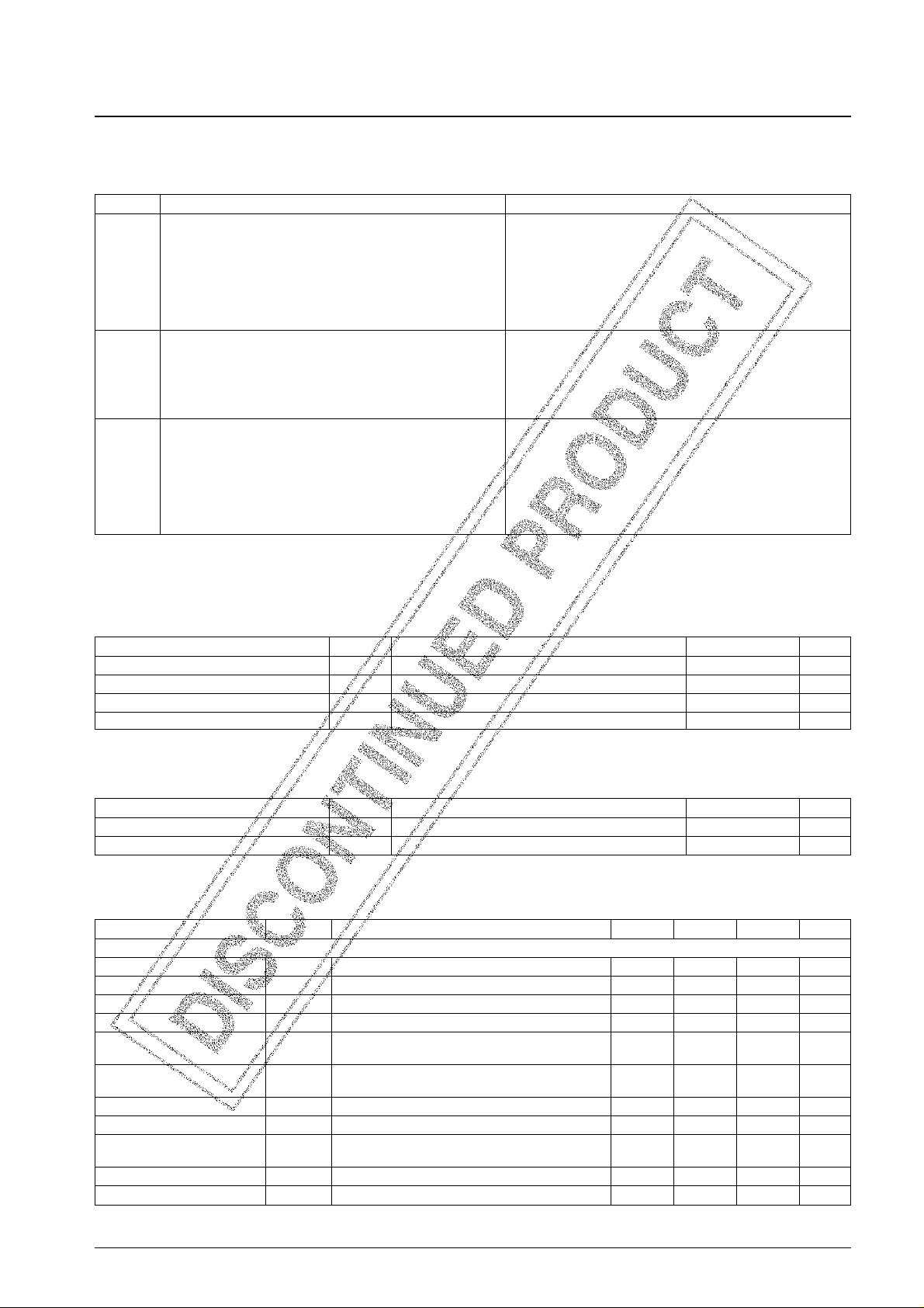
Parameter Symbol Conditions Ratings Unit
Maximum supply voltage V
CC
max 7.0 V
Allowable power dissipation Pd max Ta ≤ 65°C 1070 mW
Operating temperature Topr –10 to +65 °C
Storage temperature Tstg –40 to +150 °C
Parameter Symbol Conditions Ratings Unit
Recommended supply voltage V
CC
5.0 V
Operating supply voltage range V
CC
op 4.8 to 5.5 V
Parameter Symbol Conditions min typ max Unit
[Record Mode Y System]
Record mode current drain I
CCR
Input: 1.0 Vp-p video signal 95 120 145 mA
EE output level V
EE
The T28 output level 2.04 2.15 2.26 Vp-p
AGC characteristics 1 AGC1 With the input level increased 6 dB 0 0.5 1.0 dB
AGC characteristics 2 AGC2 With the input level decreased 6 dB –1.0 –0.3 0 dB
AGC characteristics 3 AGC3
Input: with only the sync level increased 6 dB,
540 600 660 mVp-p
measure the T28 sync level.
AGC characteristics 4 AGC4
Input: with only the sync level decreased 6 dB,
370 410 450 mVp-p
measure the T28 sync level.
Sync separator output level V
SYR
The T26 output pulse peak value 4.0 4.4 4.6 Vp-p
Sync separator output pulse width PW
SYR
The T26 output pulse width 4.1 4.4 4.7 µs
Sync separator output leading
∆T
SYR
0.8 1.0 1.2 µs
edge delay time
Sync separator threshold level TH
SYR
–23 –19 dB
VCA detection voltage V
VCA
3.00 3.20 3.40 V
Continued on next page.
Page 3
Continued from preceding page.
No. 5110-3/7
LA7425
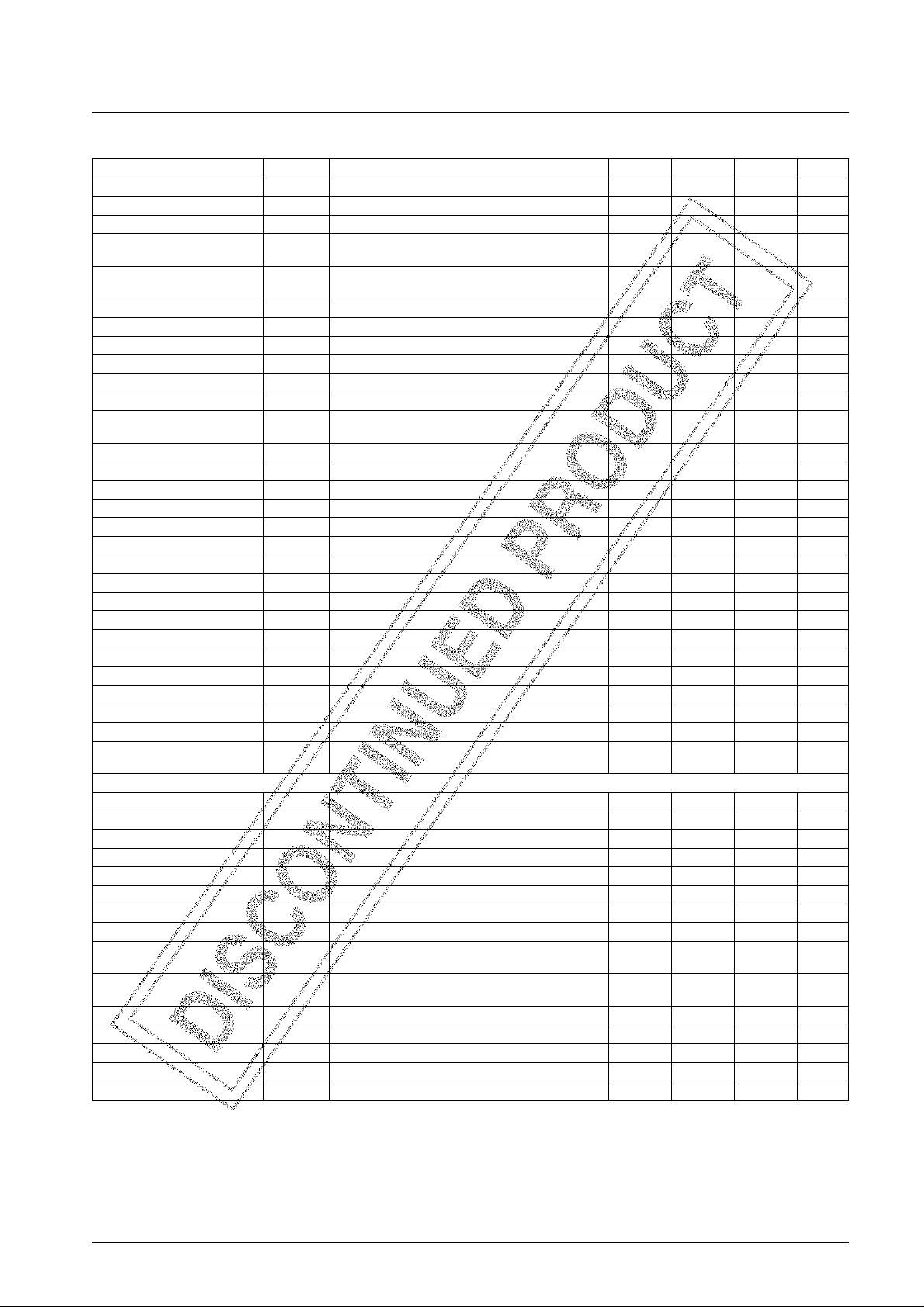
Parameter Symbol Conditions min typ max Unit
Y comb characteristics G
Y-COMB
Input: chroma noise test signal 1 Vp-p, measure T2. –25 dB
C comb characteristics G
C-COMB
Input: white 50% plus CW 3 MHz, measure T21. –25 dB
Record YNR operation EP/LP R-YNR 10 12 14 mV
CCD front-end LPF frequency
PFIL1 The attenuation at 4 MHz referenced to 500 kHz 0 0.5 1.0 dB
characteristics 1
CCD front-end LPF frequency
PFIL2 The attenuation at 10 MHz referenced to 500 kHz –17 –15 –13 dB
characteristics 2
Y LPF frequency characteristics 1 YLPF1 The attenuation at 1 MHz referenced to 500 kHz –0.5 0 +0.5 dB
Y LPF frequency characteristics 2 YLPF2 The attenuation at 2 MHz referenced to 500 kHz –0.5 +0.5 +1.5 dB
Y LPF frequency characteristics 3 YLPF3 The attenuation at 3 MHz referenced to 500 kHz –8 –6 –4dB
Y LPF frequency characteristics 4 YLPF4 The attenuation at 3.58 MHz referenced to 500 kHz –15 dB
Y LPF frequency characteristics 5 YLPF5 The attenuation at 4.2 MHz referenced to 500 kHz –15 dB
FM modulator output level V
FM
With no input signal 0.96 1.08 1.21 mVp-p
FM modulator output second
H
MOD
–40 –35 dB
harmonic distortion
Carrier frequency F
FM
3.30 3.40 3.50 MHz
Deviation FM
DEV
0.95 1.00 1.05 MHz
FM modulator linearity L
MOD
T3 = 2.6 V, 2.85 V, 3.1 V –2 0 +2 %
1/2 f
H
carrier shift CS 6.8 7.8 9.5 kHz
Emphasis gain G
EMPH
Input: 0.5 Vp-p 10 kHz sine wave –0.5 0 +0.5 dB
Detail enhancer characteristics 1 G
ENH1
Input: –10 dB, 2 MHz 1.6 1.9 2.6 dB
Detail enhancer characteristics 2 G
ENH2
Input: –20 dB, 2 MHz 3.1 4.1 5.1 dB
Detail enhancer characteristics 3 G
ENH3
Input: –30 dB, 2 MHz 5.3 6.3 7.3 dB
Detail enhancer characteristics 4 G
ENH4
Input: –30 dB, 2 MHz, edit mode 2.9 3.9 4.9 dB
NL emphasis characteristics 1 G
NLEMP1
Input: 500 mVp-p, 2 MHz 0.5 1.4 2.3 dB
NL emphasis characteristics 2 G
NLEMP2
Input: –10 dB, 2 MHz 2.6 3.8 5.2 dB
NL emphasis characteristics 3 G
NLEMP3
Input: –20 dB, 2 MHz 4.9 6.4 7.9 dB
Main emphasis characteristics 1 G
ME1
Input: –20 dB, 200 kHz 4.9 5.2 5.5 dB
Main emphasis characteristics 2 G
ME2
Input: –20 dB, 2 MHz 13.1 13.6 14.1 dB
White clipping level L
WC
Input: 1.0 Vp-p white 100% video signal 180 190 200 %
Dark clipping level L
DC
Input: 1.0 Vp-p white 100% video signal –55 –50 –45 %
Synchronization detector
V
SYDET
2.7 3.0 3.3 V
output level
[Playback Mode Y System]
Playback mode current drain I
CCP
120 150 180 mA
FM equalizer characteristics 1 G
FM-EQ1
Input: 300 mVp-p, 4 MHz –1.0 +1.0 +3.0 dB
FM equalizer characteristics 2 G
FM-EQ2
Input: 300 mVp-p, 629 kHz –30 dB
Dropout compensation period T
DOC
81012H
DOC loop gain G
DOC
5H later –1.0 0 +1.0 dB
Playback Y level V
Y-OUT
2.04 2.15 2.26 Vp-p
FM demodulator linearity L
DEM
2, 4, 6 MHz –3.5 0 +3.5 %
Demodulator carrier leakage CL Input: 4 MHz, 300 mVp-p –40 –35 dB
Playback YNR characteristics 1
P-YNR1 Input: white 50% plus CW –9 –8 –7dB
(LP/EP)
Playback YNR characteristics 2
P-YNR2 Input: white 50% plus CW –4.5 –3.5 –2.5 dB
(SP)
NL de-emphasis characteristics 1 G
NLDEEM1
Input: –10 dB, 2 MHz –6.0 –5.0 –4.0 dB
NL de-emphasis characteristics 2 G
NLDEEM2
Input: –20 dB, 2 MHz –9.0 –8.0 –7.0 dB
Noise canceller characteristics 1 G
WNC1
Input: –10 dB, 1.2 MHz –2.7 –2.2 –1.7 dB
Noise canceller characteristics 2 G
WNC2
Input: –20 dB, 1.2 MHz –7 –6 –5dB
Noise canceller characteristics 3 G
WNC3
Input: –30 dB, 1.2 MHz –13 –11 –9dB
Continued on next page.
Page 4

Continued from preceding page.
No. 5110-4/7
LA7425
Parameter Symbol Conditions min typ max Unit
Picture control hard response
G
PH1
Input: –10 dB, 1 MHz 1.0 1.5 2.0 dB
characteristics 1
Picture control hard response
G
PH2
Input: –10 dB, 2 MHz 3.2 4.2 5.2 dB
characteristics 2
Picture control soft response
G
PS1
Input: –10 dB, 1 MHz –6.0 –5.0 –4.0 dB
characteristics 1
Picture control soft response
G
PS2
Input: –10 dB, 2 MHz –12.0 –10.0 –8.0 dB
characteristics 2
Quasi-V insertion level (playback) ∆VD
P
V29= 5 V –80 0 +80 mV
Quasi-H insertion level (playback) ∆HD
P
V29= 2.5 V –200 –100 0 mV
Sync separator output level V
SYP
Pin 26 output pulse peak value 4.0 4.4 4.6 Vp-p
Sync separator output pulse width PW
SYP
Pin 26 output pulse width 4.3 4.6 4.9 µs
Sync separator output leading
∆T
SYP
1.25 1.45 1.65 µs
edge delay time
Built-in regulator voltage V
REG
3.9 4.1 4.3 V
S-VHS discriminator output level V
SVHSP
2.7 3.0 3.3 V
[Record Mode Chroma System]
Y/C separator output burst level V
OR-21
Pin 21 burst level 120 150 180 mVp-p
Chroma low frequency
V
OR-14
Input: standard color bar signal 1 Vp-p 322 380 438 mVp-p
conversion burst level
Burst emphasis G
BE
5.5 6.0 6.5 dB
VXO oscillator level V
VXO-R
Input: standard color bar signal 1 V p-p 400 500 600 dB
ACC characteristics 1 ACC
R1
With only the color signal level increased 6 dB +0.2 +0.5 dB
ACC characteristics 2 ACC
R2
With only the color signal level decreased 6 dB –0.5 –0.1 dB
ACC killer on input level V
IN-ACCK-ON
–29 –26 –23 dB
ACC killer on output level V
O-ACCK
–60 –50 dB
ACC killer recovery input level
V
IN-ACCK-OFF
–23 –20 –17 dB
APC pull-in range 1 ∆f
APC1
+350 +480 Hz
APC pull-in range 2 ∆f
APC2
–770 –350 Hz
AFC pull-in range 1 ∆f
AFC1
+1.0 +3.0 kHz
AFC pull-in range 2 ∆f
AFC2
–2.5 –1.0 kHz
Record Y/C level ratio C/FM –9.9 –9.1 –8.3 dB
[Playback Mode Chroma System]
Video output burst level V
OP-28
SP mode, input burst 160 mVp-p 235 277 319 mVp-p
Pin 21 output burst level V
OP-21
SP mode, input burst 160 mVp-p 149 175 201 mVp-p
ACC characteristics 1 ACC
P1
With the input chroma level increased 6 dB 0.5 0.8 dB
ACC characteristics 2 ACC
P2
With the input chroma level decreased 6 dB –0.5 –0.2 dB
Killer on input level V
ACK-P
–55 –40 dB
Killer on chroma output level V
OACKP
–44 –40 dB
Main converter carrier leakage C
LP
The 4.21 MHz carrier leakage component –40 –33 dB
4.84 MHz spurious signal level SPR
484
–35 dB
Burst de-emphasis G
BD
–5.35 –5.10 –4.85 dB
XO output level V
XO-P
370 470 570 mVp-p
XO oscillator frequency deviation ∆f
XO
∆fXO= f – 3579545 (Hz) –70+7Hz
Page 5

Test Circuit
No. 5110-5/7
LA7425
Page 6

Control Pin Function Table
Note: Do not set pin 12 to a voltage of 1.5 V or lower, since the chip will enter test mode.
Mode Control Table
Note: CNR is not turned off in edit mode.
* The APC loop becomes post-comb when pin 16 is set high (trick mode).
No. 5110-6/7
LA7425
Pin No. Control function L M H
REC
Synchronization detector output when open. 3.6 V or higher
1
CNR adjustment
(0 V when synchronized, 3.0 V when not synchronized) CNR adjustment mode
Forced NVHS control
PB
S-VHS detector output when open. 3.6 V or higher
(0 V in normal mode, 3.0 V for S-VHS) Forced N-VHS mode
4 Record/playback switching
Open 3.8 V or higher
Record mode Playback mode
7 SP/LP/EP switching
1.2 V or lower 1.8 to 2.7 V 3.3 V or higher
SP mode LP mode EP mode
11
If a 3.3 kΩ resistor is connected between pin 11 and ground, the playback mode SP YNR will be set to
strong (K = 0.5), and to very strong (K = 0.6) in LP/EP modes.
12 Edit/picture control
2 to 2.5 V 2.5 to 3 V 3.6 V or higher
Picture control: soft Picture control: hard Edit mode
Noise canceller control 1.5 V or lower 2.0 to 3.0 V
3.8 V or higher
13
Y/C mix off Noise canceller: off Noise canceller linear control
Y/C mix: off
(playback Y/C separate output)
16
APC loop switching 3.8 V or higher (200 µA or higher)
(trick mode) APC loop “post-comb”
21
3.5 V or higher
Record: XO: forced free-run
23 CNR control
1.5 V or lower Open 2.5 V or higher
*** CNR: on CNR: off
29 QV/QH insertion
0.8 V or lower 1.0 to 2.2 V 2.5 to 3.2 V 3.8 V or higher
Through Character insertion QH insertion QV insertion
30 Rotary pulse input
1.2 V or lower 1.8 V or higher
Low CH High CH
34 DOC stop control
Open 3.75 V or higher
Normal mode DOC stopped
SP EP LP
Normal Edit Normal Edit Normal Edit
Detail enhancer Strong Weak Weak Weak Weak Weak
YNR
K — 0.65
LIMITT — 5 IRE
REC Y/C comb separator
CO— O — O —
YO
1/2 f
H
carrier shift — O
Nonlinear emphasis — O
Burst emphasis O —
YNR
K 0.2 0.5 0.2 0.5 0.2
LIMITT 5 IRE 11 IRE 5 IRE 11 IRE 5 IRE
Picture control O Center point O Center point O Center point
PB
Burst de-emphasis O —
Crosstalk cancellation
O —
correlation switching
APC loop Pre-comb
*
Post-comb
Four phase shift clock DPLL output HHK output
Page 7

PS No. 5110-7/7
LA7425
Block Diagram
This catalog provides information as of May, 1995. Specifications and information herein are subject to change
without notice.
■ No products described or contained herein are intended for use in surgical implants, life-support systems, aerospace
equipment, nuclear power control systems, vehicles, disaster/crime-prevention equipment and the like, the failure of
which may directly or indirectly cause injury, death or property loss.
■ Anyone purchasing any products described or contained herein for an above-mentioned use shall:
➀ Accept full responsibility and indemnify and defend SANYO ELECTRIC CO., LTD., its affiliates, subsidiaries and
distributors and all their officers and employees, jointly and severally, against any and all claims and litigation and all
damages, cost and expenses associated with such use:
➁ Not impose any responsibility for any fault or negligence which may be cited in any such claim or litigation on
SANYO ELECTRIC CO., LTD., its affiliates, subsidiaries and distributors or any of their officers and employees
jointly or severally.
■ Information (including circuit diagrams and circuit parameters) herein is for example only; it is not guaranteed for
volume production. SANYO believes information herein is accurate and reliable, but no guarantees are made or implied
regarding its use or any infringements of intellectual property rights or other rights of third parties.
 Loading...