

SANYO LA7415 Datasheet
Monolithic Linear IC
No. 5647
VHS VCR Playback Head and Record Amplifiers
Overview
The LA7415 is a record and playback amplifier IC for
VHS format VCR decks. In combination with a Sanyo
LC7420 or LA7430 Series video signal processing IC, the
LA7415 can provide an adjustment-free Y/C record
current.
Features
• Record amplifier: Provides stable recording
characteristics using a fixed-current drive technique that
is resistant to load variations.
• REC-AMP: Includes a built-in AGC circuit.
• Can use the same printed circuit board as the LA7411.
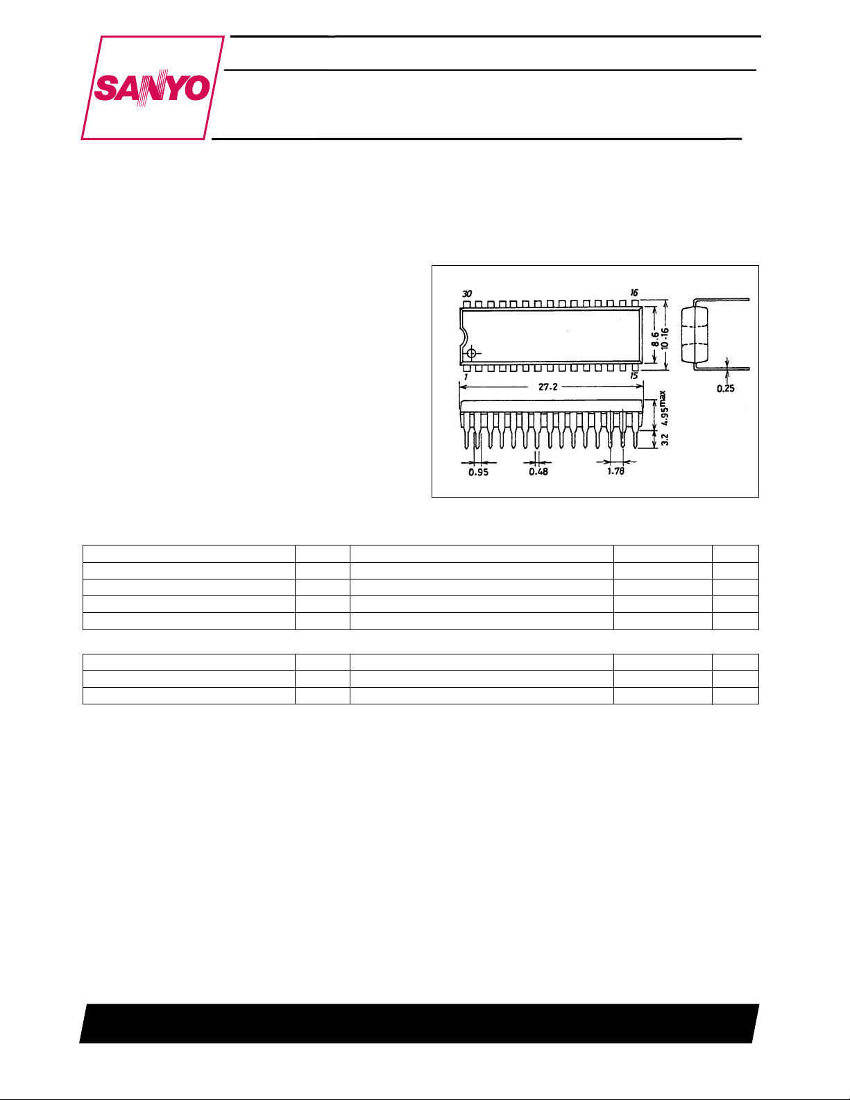
LA7415
Package Dimension
unit: mm
3061-DIP30S
[LA7415]
SANYO: DIP30S
Specifications
Maximum Ratings at Ta = 25°C
Parameter Symbol Conditions Ratings Unit
Maximum supply voltage V
Allowable power dissipation Pd max Ta ≤ 65 °C 650 W
Operating temperature Topr –10 to +65 °C
Storage temperature Tstg –40 to +150 °C
Operating Conditions at Ta = 25°C
Parameter Symbol Conditions Ratings Unit
Supply voltage V
Operating voltage range V
max 7.0 V
CC
CC
op 4.8 to 5.5 V
CC
5.0 V
SANYO Electric Co.,Ltd. Semiconductor Bussiness Headquarters
TOKYO OFFICE Tokyo Bldg., 1-10, 1 Chome, Ueno, Taito-ku, TOKYO, 110 JAPAN
43097HA(OA) No. 5647-1/12
LA7415
Electrical Characteristics at Ta = 25°C
Ratings
Parameter Symbol Conditions
Input Output T2 T4 T5
[Playback Mode]
Current drain I
SP L CH1 VG
Voltage gain
SP H CH2 VG
EP L CH3 VG
EP H CH4 VG
Voltage gain differential 1 ∆VG
Voltage gain differential 2 ∆VG
Inter-mode gain difference ∆
Equivalent input CH2 V
noise voltage CH3 V
CH1 V
CH4 V
CCP
1 T20A T10A OPEN 0 0 54.0 57.0 60.0 dB
P
2 T23A T10A
P
3 T27A T10A
P
4 T30A T10A OPEN 5.0 2.5 56.0 59.0 62.0 dB
P
1– –VGP1 – VGP2––––10+1dB
P
2– –VGP3 – VGP4––––10+1dB
P
VG
NIN
NIN
NIN
NIN
––VGP3 – VGP1–––123dB
P EP-SP
1 T20A T10A
2 T23A T10A
3 T27A T10A
4 T30A T10A OPEN 5.0 2.5 – 1.1 1.5 µVrms
CH1 ∆Vfp1 T20A T10A
Frequency CH2 ∆Vfp2 T23A T10A
characteristics CH3 ∆Vfp3 T27A T10A
CH4 ∆Vfp4 T30A T10A
CH1 V
Second harmonic CH2 V
distortion CH3 V
CH4 V
CH1 V
Maximum CH2 V
output level CH3 V
CH4 V
1 T20A T10A
HDP
2 T23A T10A
HDP
3 T27A T10A
HDP
4 T30A T10A
HDP
1 T20A T10A
OMP
2 T23A T10A
OMP
3 T27A T10A
OMP
4 T30A T10A OPEN 5.0 2.5 1.0 1.2 – Vp-p
OMP
T15: 5.0 V, T13: OPEN, TRCK HA SW30
T7: OPEN MUTE
Pin 15 influx current OPEN 0 0 24 30 36 mA
= 38 mVp-p,
V
IN
f = 1 MHz
After the 1.1-MHz LPF
V
OUT
VG
1, 2, 3, 4
P
V
= 38 mVp-p
IN
f = 7 MHz
V
OUT
1, 2, 3, 4 output ratio
VG
P
V
= 38 mVp-p
IN
f = 4 MHz
(8-MHz component)/(4-MHz component)
output ratio
f = 1 MHz
The output level when the third
harmonic in the output is –30 dB
OPEN 0 2.5 54.0 57.0 60.0 dB
OPEN 5.0 0 56.0 59.0 62.0 dB
OPEN 0 0 – 1.1 1.5 µVrms
OPEN 0 2.5 – 1.1 1.5 µVrms
OPEN 5.0 0 – 1.1 1.5 µVrms
OPEN 0 0 –2.5 0 – dB
OPEN 0 2.5 –2.5 0 – dB
OPEN 5.0 0 –2.5 0 – dB
OPEN 5.0 2.5 –2.5 0 – dB
OPEN 0 0 – –40 –35 dB
OPEN 0 2.5 – –40 –35 dB
OPEN 5.0 0 – –40 –35 dB
OPEN 5.0 2.5 – –40 –35 dB
OPEN 0 0 1.0 1.2 – Vp-p
OPEN 0 2.5 1.0 1.2 – Vp-p
OPEN 5.0 0 1.0 1.2 – Vp-p
T23A T10A OPEN 0 0 – –40 –35 dB
CH1 V
Crosstalk SP T30A T10A
(Note 1) T20A T10A
CH2 V
1 T27A T10A
CR
2 T27A T10A
CR
V
= 38 mVp-p,
IN
f = 4 MHz
V
OUT
1, 2
VG
P
OPEN 0 0 – –40 –35 dB
OPEN 0 0 – –40 –35 dB
OPEN 0 2.5 – –40 –35 dB
OPEN 0 2.5 – –40 –35 dB
T30A T10A OPEN 0 2.5 – –40 –35 dB
T23A T10A OPEN 5.0 0 – –40 –35 dB
CH3 V
Crosstalk EP T30A T10A
(Note 1) T20A T10A
CH4 V
3 T27A T10A
CR
4 T27A T10A
CR
V
= 38 mVp-p,
I
f = 4 MHz
V
OUT
3, 4
VG
P
OPEN 5.0 0 – –40 –35 dB
OPEN 5.0 0 – –40 –35 dB
OPEN 5.0 2.5 – –40 –35 dB
OPEN 5.0 2.5 – –40 –35 dB
T30A T10A OPEN 5.0 2.5 – –40 –35 dB
∆V
1 – T10 CH1-CH2
ODC
∆V
2 – T10 CH3-CH4
ODC
∆V
3 – T10 CH1-CH3
Output DC OPEN 5.0 0 –100 0 +100 mV
offset
ODC
∆V
4 – T10 CH2-CH4
ODC
∆V
5 – T10 CH1-CH4
ODC
∆V
6 – T10 CH2-CH3
ODC
OPEN – 0 –100 0 +100 mV
OPEN 0 2.5 –100 0 +100 mV
OPEN – 0 –100 0 +100 mV
OPEN 5.0 2.5 –100 0 +100 mV
OPEN 0 – –100 0 +100 mV
OPEN 0 – –100 0 +100 mV
OPEN 5.0 2.5 –100 0 +100 mV
OPEN 0 0 –100 0 +100 mV
OPEN 5.0 2.5 –100 0 +100 mV
OPEN 0 2.5 –100 0 +100 mV
OPEN 5.0 0 –100 0 +100 mV
Note 1. With the input inductor L (8.2 µH) shorted.
Since the T4 (HA) control switch timing is synchronized with T6 (H-Sync), a T6 trigger (0 - 5 V - 0) must be input before measuring each of these items.
2.
min typ max
Continued on the next page.
Unit
No. 5647-2/12
LA7415
Continued from the preceding page.
Parameter Symbol Conditions
Input Output T2 T4 T5
T15: 5.0 V, T13: OPEN, TRCK HA SW30
T7: OPEN MUTE
Enveloped detector
output pin voltage
Enveloped detector
voltage SP1 T10A: Adjusted to 300 mV p-p
Enveloped detector
voltage SP2 T10A: Adjusted to 600 mV p-p
Enveloped detector
voltage EP1 T10A: Adjusted to 200 mV p-p
Enveloped detector
voltage EP2 T10A: Adjusted to 450 mV p-p
Comparator
output voltage 1 The T3 DC voltage
Comparator
output voltage 2 The T3 DC voltage
Playback mode on switching
transistor on resistance
Playback mode
mode switching
transistor on
resistance
Trick 1 threshold
level
Trick 2 threshold
level
HAPB threshold
level
SW30 threshold
level
[Record Mode]
Current drain I
AGC amplifier
output level
Inter-mode gain
difference
AGC amplifier control
characteristics 1
AGC amplifier control
characteristics 2
AGC amplifier frequency
characteristics
AGC amplifier second
harmonic distortion
AGC amplifier maximum
output level
AGC amplifier muting
attenuation
V
ENV
V
ENVSP1
V
ENVSP2
V
ENVEP1
V
ENVEP2
V
COMP1
V
COMP2
R
17 P-17
PON
18 P-18
R
PON
21 P-21 OPEN 5.0 – – 4.0 6.0 Ω
R
PON
R
24 P-24
PON
26 P-26
R
PON
29 P-29 OPEN 0 – – 4.0 6.0 Ω
R
PON
T8 The T8 DC voltage with no input OPEN 0 0 0 0.4 0.8 V
T20A T8
T20A T8
T27A T8
T27A T8
T20A T3
T20A T3
f = 4 MHz
f = 4 MHz
f = 4 MHz
f = 4 MHz
f = 4 MHz, V
f = 4 MHz, V
= 38 mVp-p
IN
= 38 mVp-p
IN
The difference in the DC measurement
for 1-mA and 2-mA influx currents
The difference in the DC measurement
for 1-mA and 2-mA influx currents
TR1-1 T2 Normal → Trick1 * – – 3.2 – 5.0 V
TR1-2 T2 Trick1 → Normal * – – 1.2 – 2.8 V
TR2-1 T2 Normal → Trick2 * – – 0.0 – 0.8 V
TR2-2 T2 Trick2 → Normal * – – 1.2 – 2.8 V
HAP-1 T4 SP → EP – * – 1.8 – 5.0 V
HAP-2 T4 EP → SP – * – 0.0 – 1.4 V
SW30-1 T5 Lch → Hch – – * 1.2 – 5.0 V
SW30-2 T4 Hch → Lch – – * 0.0 – 0.8 V
T15: 5.0 V, T2: OPEN, REC HA SW30
T6: 5.0 V, T7: 5.0 V Adj2 MUTE
The pin 15 influx current OPEN 0 0 44 55 66 mA
f = 4 MHz
V
= 200 mVp-p
IN
RSP/VREP
f = 4 MHz, V
The output level/V
f = 4 MHz, V
The output level/V
f = 1 MHz, 7 MHz, VIN= 100 mVp-p
The 7 MHz/1 MHz output ratio
f = 4 MHz, V
= 400 mVp-p
IN
RSP, EP
= 100 mVp-p
IN
RSP, EP
= 200 mVp-p
IN
The (8 MHz component)/(4 MHz component)
output ratio
f = 4 MHz, The output level for which
the second harmonic is –35 dB
f = 4 MHz, VI = 200 mVp-p
The output level/V
RSP, EP
∆
∆
∆
∆
∆V
∆V
∆V
∆V
V
V
∆VG
V
AGC
V
AGC
V
AGC
V
AGC
∆V
∆V
∆V
∆V
CCR
RSP
REP
FRS
FRE
HDRS
HDRE
OMRS
OMRE
MRS
MRE
T11A T21A
T11A T26A
––V
R
1-SP
T11A T21A
1-EP
T11A T26A
2-SP
T11A T21A
2-EP
T11A T26A
T11A T21A
T11A T26A
T11A T21A
T11A T21A
T11A T21A
T11A T26A
T11A T21A
T11A T26A
ratio
ratio
ratio
Ratings
min typ max
Unit
OPEN 0 0 2.1 2.6 3.1 V
OPEN 0 0 4.5 4.8 5.0 V
OPEN 5.0 0 2.0 2.6 3.0 V
OPEN 5.0 0 4.5 4.8 5.0 V
5.0 0 0 – 0.4 0.7 V
5.0 5.0 0 4.5 4.8 – V
– – – – 4.0 6.0 Ω
– – – – 4.0 6.0 Ω
OPEN 5.0 – – 4.0 6.0 Ω
OPEN 0 – – 4.0 6.0 Ω
T2 T4 T5
OPEN 0 0 147 156 165 mVp-p
OPEN 5.0 0 116 123 130 mVp-p
– – – 1.30 2.05 2.80 dB
OPEN 0 0 – 0.5 1.0 dB
OPEN 5.0 0 – 0.5 1.0 dB
OPEN 0 0 –1.0 –0.5 – dB
OPEN 5.0 0 –1.0 –0.5 – dB
OPEN 0 0 –1.0 –0.0 +1.0 dB
OPEN 5.0 0 –1.0 –0.0 +1.0 dB
OPEN 0 0 – –45 –40 dB
OPEN 5.0 0 – –45 –40 dB
Adj. 0 0 20 22 – mAp-p
Adj. 5.0 0 20 22 – mAp-p
OPEN 0 5.0 – –45 –40 dB
OPEN 5.0 5.0 – –45 –40 dB
Continued on the next page.
No. 5647-3/12
Continued from the preceding page.
Parameter Symbol Conditions
[Record Mode]
LA7415
Input Output T2 T4 T5
T15: 5.0 V, T2: OPEN, REC HA SW30
T6: 5.0 V, T7: 5.0 V Adj2 MUTE
Ratings
min typ max
Unit
AGC amplifier
relative cross
modulation level
Record mode
mode switching
transistor on
resistance
HA record
threshold level
Record MUTE
threshold level
Record/playback
threshold level
Notes 3. Measure with a DC voltage of about 1.8 V applied to the AGC detector filter pin (pin 12) and with the AGC amplifier gain fixed.
4. Adjust the output level by applying a DC voltage to T13 (REC CUR.Adj2)
5. Use a resistor with a ±1.0% tolerance between pins 14 and 15.
∆V
∆V
R
R
R
R
R
R
HAR-1 T4 SP → EP – *–1.8 – 5.0 V
HAR-2 T4 EP → SP – *–0.0 – 1.4 V
MUTE-1 T5 MUTE OFF → ON – – * 3.4 – 5.0 V
MUTE-2 T5 MUTE ON → OFF – – * 0.0 – 3.0 V
SW REC/PB
T10A T21A
CYS
T11A T26A
CYE
17 P-17 OPEN 5.0 – – 4.0 6.0 Ω
RON
18 P-18
RON
21 P-21
RON
24 P-24
RON
26 P-26 OPEN 0 – – 4.0 6.0 Ω
RON
29 P-29 OPEN 0 – – 4.0 6.0 Ω
RON
T10A: f = 629 kHz, VIN= 360 mVp-p
T11A: f = 4 MHz, VIN= 200 mVp-p
(4 MHz ±629 kHz)/(4 MHz)
output ratio
The difference in the DC
measurement for 1-mA
and 2-mA influx currents
T7: control voltage – – – 2.2 – 5.0 V
OPEN 0 0 – –45 –40 dB
OPEN 5.0 0 – –45 –40 dB
OPEN 0 – – 4.0 6.0 Ω
OPEN 5.0 – – 4.0 6.0 Ω
OPEN 5.0 – – 4.0 6.0 Ω
Usage Notes
1. Control Pin Logic
RF SW, REC MUTE: pin 5
Record/playback mode switching: pin 7
Playback mode
If the pin 5 DC voltage is < 1.0 V: Lch
If the pin 5 DC voltage is > 1.0 V: Hch
Record mode
If the pin 5 DC voltage is < 3.2 V: Muting will be off
If the pin 5 DC voltage is > 3.2 V: Muting will be on
If the pin 7 DC voltage is < 2.0 V: Playback mode
If the pin 7 DC voltage is > 2.0 V: Record mode
No. 5647-4/12
 Loading...