

Sanyo LA7391AN Specifications

Ordering number: EN 3951B
Monolithic Linear IC
LA7391AN
Global VHS-format VCR
Video Signal Processor
Overview
The LA7391AN is a multi-format, single-chip video signal
processing IC that supports TV systems around the world.
Features
.
Compatible with TV systems around the world (NTSC/
PAL/MESECAM/4.43 -NTSC/PAL-M/PAL-N).
.
All filters on chip, except for PB-LPF for chroma (cutoff
frequency requires no adjustment).
.
No adjustment of YNR and DOC levels.
.
Double high-pass noise canceller on chip.
.
Linear phase-type picture control on chip.
.
fsc output can be used as clock for OSD IC.
.
DCC circuit on chip.
.
Pilot burst erasure circuit on chip.
.
High-speed AFC circuit on chip.
.
Switching noise canceller on chip.
.
Smallest package in the industry.
.
Few components needed.
.
2fsc output.
Specifications
Maximum Ratings atTa=25°C
Package Dimensions
unit: mm
3025B-DIP42S
42
1
.
I/O pin for CNR insertion added.
.
YNR/LNC switching possible.
[LA7391AN]
37.9
22
13.8
15.24
21
4.25
5.1max
3.8
0.51min
1.15
1.780.480.95
SANYO : DIP42S
0.25
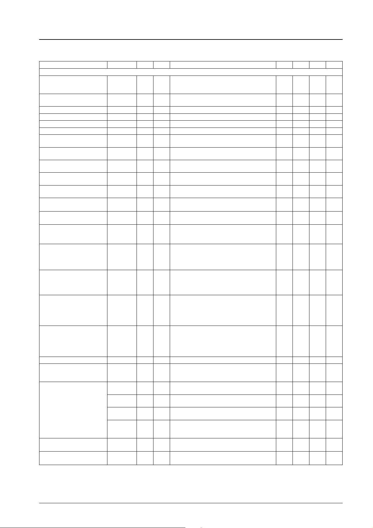
Parameter Symbol Conditions Ratings Unit
Maximum supply voltage V
Allowable power dissipation Pdmax Ta %65°C 1020 mW
Operating temperature Topr –10 to +65
Storage temperature Tstg –40 to +150
max 7.0 V
CC
Operating Conditions atTa=25°C
Parameter Symbol Conditions Ratings Unit
Recommended supply voltage V
Operating supply voltage range V
Any and all SANYO products described or contained herein do not have specifications that can handle
applications that require extremely high levels of reliability, such as life-support systems, aircraft’s
control systems, or other applications whose failure can be reasonably expected to result in serious
physical and/or material damage. Consult with your SANYO representative nearest you before using
any SANYO products described or contained herein in such applications.
SANYO assumes no responsibility for equipment failures that result from using products at values that
exceed, even momentarily, rated values (such as maximum ratings, operating condition ranges, or other
parameters) listed in products specifications of any and all SANYO products described or contained
herein.
CC
op 4.8 to 5.5 V
CC
5.0 V
SANYO Electric Co.,Ltd. Semiconductor Company
TOKYO OFFICE Tokyo Bldg., 1-10, 1 Chome, Ueno, Taito-ku, TOKYO, 110-8534 JAPAN
51595TH (II) No.3951-1/11
C
°
C
°
LA7391AN
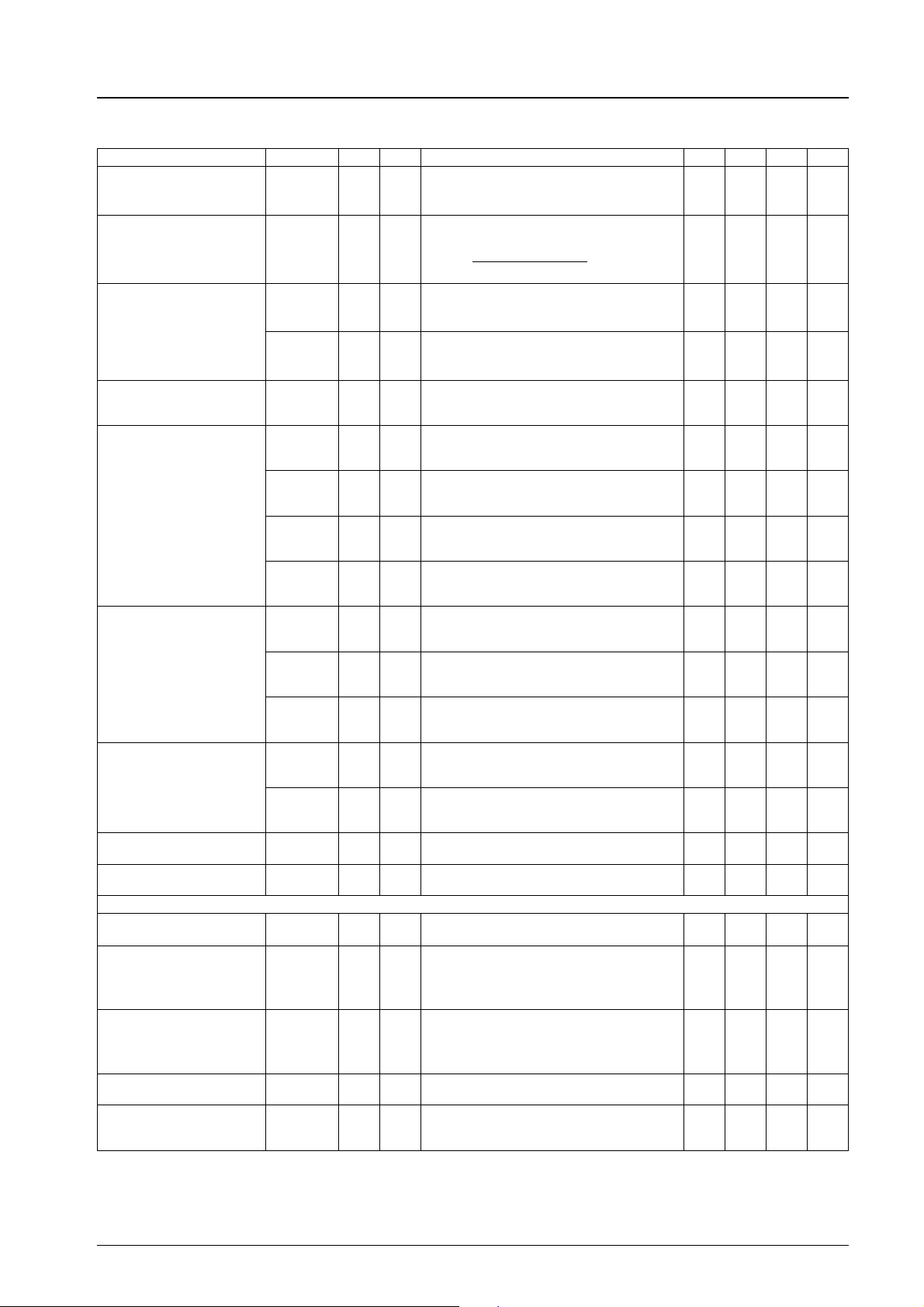
Operating Characteristics atTa=25°C, VCC= 5.0 V
Parameter Symbol Input
Output
Conditions min typ max Unit
[REC Mode Y]
Current drain REC I
CCR
When VCC= 5 V (when there is no signal),
measure sum of incoming current at pins 35
95 120 145 mA
and 28
AGC adjustment C
AGC
T37A VIN= 1.0 Vp-p video signal, use VR39 to
adjust T4 output to 0.5 Vp-p
VCA control characteristics VCA T37A T4 Measure T4 output level when S10 is set to 2 0.48 0.5 0.52 Vp-p
AGC adjustment voltage V
AGC
AGC detection voltage V
EE output level V
AGC Output 1 AGC 1 T37A T4 V
AGC Output 2 AGC 2 T37A T4 V
AGC Output 3 AGC 3 T37A T4 V
AGC Output 4 AGC 4 T37A T4 V
Sync separation output level V
Sync separation output
SYR
PW
pulse width
Sync separation output
∆ T
leading edge delay time
Sync separation threshold
TH
level
T37A T39 Measure T39 DC voltage in above state 3.2 3.4 3.6 V
T37A T38 Measure T38 DC voltage in same manner 1.2 1.4 1.6 V
AD
T37A T34A Measure T34A output level in same manner 0.95 1.00 1.05 Vp-p
EE
T37A T32 VIN= 1.0 Vp-p video signal,
= 2.0 Vp-p video signal
IN
Measure T4 output level
= 0.5 Vp-p video signal
IN
Measure T4 output level
= 700 mVp-p LUMI, 600 mVp-p SYNC
IN
Measure T4 SYNC level
= 700 mVp-p LUMI, 150 mVp-p SYNC
IN
Measure T4 SYNC level
500 540 560 mVp-p
470 490 500 mVp-p
135 150 165 mVp-p
70 85 100 mVp-p
4.0 4.2 4.4 Vp-p
Measure T32 output pulse wave high value
T37A T32 VIN= 1.0 Vp-p video signal,
SYR
T37A T32 VIN= 1.0 Vp-p video signal, measure delay
SYR
T37A T32 Gradually attenuate the input level, measure
SYR
Measure T32 output pulse width
time of output SYNC versus input SYNC
input level at point when output pulse width
4.4 4.7 5.0 µs
0.6 0.8 1.0 µs
–18 –14 dB
widens 1 µs or more beyond PWSYR
Sync tip level,
pedestal level,
white level measurement
(REC)
Pseudo V insertion level
(REC)
Pseudo H insertion level
(REC)
White insertion level (REC) ∆ WHR T37A T34 Measure T34 DC voltage when 1.3 V is
L
VOR
T37A T34 Measure electric potential for each of the T34
video output sync tip, pedestal, and white
peak, and assign the measured values to
L
SYN,LPED
, and L
, respectively
WHI
∆ VDR T37A T34 Measure T34 DC voltage when5Visapplied
to T33, and assign the measured value to
L
and calculate the difference with L
VDR
∆VDR=L
SYN–LVDR
SYN
∆ HDR T37A T34 Measure T34 DC voltage when 2.7 V is
applied to T33, and assign the measured
value to L
with L
PED
∆HDR=L
and calculate the difference
HDR
PED–LHDR
–80 0 80 mV
–200 –100 0 mV
150 250 350 mV
applied to T33, and assign the measured
VCA detection voltage V
REC YNR operation
VR-YNR T37A T3 V
EP/LP
Y-LPF frequency
YLPF 1 T37A T3 V
characteristics
YLPF2 T37A T3 V
YLPF3 T37A T3 V
YLPF4 T37A T3 V
VCA
value to L
with L
WHI
∆WHR=L
T37A T9 Measure T9 DC voltage 3.1 3.4 3.7 V
= white 50% + CW
IN
(15.8 mVp-p) ratio between 32f
and 32.5f
= standard multiburst signal 1 Vp-p,
IN
2 MHz response to 500 kHz at T3
= standard multiburst signal 1 Vp-p,
IN
4.8 MHz response to 500 kHz at T3
= standard multiburst signal 1 Vp-p,
IN
2 MHz response to 500 kHz at T3, T22A: 5 V
= standard multiburst signal 1 Vp-p,
IN
4.8 MHz response to 500 kHz at T3, T22A: 5
and calculate the difference
WHR
WHI–LWHR
component
H
component
H
3.5 4.5 5.5 dB
0.2 0.7 1.2 dB
–4.5 –3.5 –2.5 dB
0.4 0.9 1.4 dB
–5.0 –4.0 –3.0 dB
V
FM modulator output level V
FM modulator secondary
H
distortion
FM
MOD
T40 No input, use VR42 to adjust output
frequency to 4 MHz, measure output level
T40 Ratio of 8 MHz component to 4 MHz in the
above state
0.8 1.0 1.2 Vp-p
–40 –35 dB
Continued on next page.
No. 3951-2/11
Continued from preceding page.
LA7391AN
Parameter Symbol Input
FM modulator modulation
sensitivity
S
MOD
Output
Conditions min typ max Unit
T4 T40 Measure amplitude of change in output
frequency when 2.6 V DC or 3.1 V DC is
applied to T4, 2 x (f3.1 – f2.6)
FM modulator linearity L
1/2 f
carrier shift CS1 T40 Measure amplitude of change in output
H
MOD
T4 T40 Measure output frequency when 2.85 V DC
applied to T4,
L
f2.85 – (f3.1 + f2.6)/2
=
MOD
S
MOD
frequency when SW41B is off and SW41A is
switched from on to off
CS2 T40 Measure amplitude of change in output
frequency when SW41B is on and SW41A is
switched from on to off
Emphasis gain G
EMPH
T4A T5 VIN= 0.5 Vp-p 10 kHz sine wave
Measure ratio of levels of input and output
amplitude at T5
Detail enhancer
characteristics
Nonlinear emphasis
characteristics
Main linear emphasis
characteristics
White clipping level L
Dark clipping level L
G
ENH1
G
ENH2
G
ENH3
G
ENH4
G
NLEMP1
G
NLEMP2
G
NLEMP3
G
ME1
G
ME2
WC
DC
T4A T5 VIN= 158 mVp-p 2 MHz sine wave
Measure ratio of levels of T5 and T4,
difference with G
EMPH
T4A T5 VIN= 50 mVp-p 2 MHz sine wave
Measure ratio of levels of T5 and T4,
difference with G
EMPH
T4A T5 VIN= 15.8 mVp-p 2 MHz sine wave
Measure ratio of levels of T5 and T4,
difference with G
EMPH
T4A T5 VIN= 15.8 mVp-p 2 MHz sine wave
Measure output amplitude at T5 in edit mode,
difference with G
EMPH
T4A T5 VIN= 500 mVp-p 2 MHz
Measure ratio of levels of T5 and T4,
difference with G
EMPH
T4A T5 VIN= 158 mVp-p 2 MHz
Measure ratio of levels of T5 and T4,
difference with G
EMPH
T4A T5 VIN= 50 mVp-p 2 MHz
Measure ratio of levels of T5 and T4,
difference with G
EMPH
T4A T5 VIN= 50 mVp-p 200 kHz sine wave
Measure ratio of levels of T5 and T4,
difference with G
EMPH
T4A T5 VIN= 50 mVp-p 2 MHz
Measure ratio of levels of T5 and T4,
difference with G
EMPH
T4A T5 VIN= 500 mVp-p white 100% video signal
Measure white clipping level at T5
T4A T5 VIN= 500 mVp-p white 100% video signal
Measure dark clipping level at T5
[PB Mode Y]
Current drain PB I
Dropout compensation
period
P Incoming current at pins 35 and 28 when
T
CC
DOC
T39A
T4A
V
= 5.0 V
CC
T34A T39A: 4 MHz, 300 mVp-p sine wave
T4A: 0.5Vp-p video signal
T34A: time from when input went to 0 until
T34A output returned, SW10 → 1
DOC loop gain GDOC T39A
T12 T39A: 4 MHz, 300 mVp-p sine wave
T4A
T4A: 0.5Vp-p video signal
T39A: Input/output response when 5H have
elapsed after input went to 0, SW10 → 3
FM demodulation voltage V
FM demodulation sensitivity S
DEM4
DEM
T39A T3 VIN=300 mVp-p,f=4MHz, Output DC
voltage
T39A T3 VIN= 300 mVp-p,f=2MHz, V
VIN= 300 mVp-p,f=6MHz, V
Calculate S
DEM
=(V
DEM6–VDEM2
x 100
DEM2
DEM6
)/4
1.6 2.0 2.4
MHz/V
–2 0 2 %
6.8 7.8 9.5 kHz
6.8 7.8 9.5 kHz
–0.5 0 0.5 dB
0.9 1.4 1.9 dB
2.2 3.2 4.2 dB
4.0 5.0 6.0 dB
1.8 2.8 3.8 dB
0.5 1.4 2.3 dB
2.6 3.8 5.2 dB
4.9 6.4 7.9 dB
4.9 5.2 5.5 dB
13.1 13.6 14.1 dB
186 193 200 %
–60 –55 –50 %
125 155 185 mA
0.35 0.5 0.65 ms
–1.0 0 1.0 dB
1.5 2.0 2.5 V
0.36 0.45 0.54 V/MHz
Continued on next page.
No. 3951-3/11
Continued from preceding page.
LA7391AN
Parameter Symbol Input
FM demodulation linearity L
DEM
Carrier leak CL T39A T3 V
PB YNR characteristics
GP-YNR T4A T28A V
LP/EP
PB LNC characteristics
GP-LNC T4A T28A V
SP
Playback through gain G
PB
L
DEM
Output
V
DEM4
=
–(V
DEM6+VDEM2
V
DEM6–VDEM2
= 300 mVp-p,f=4MHz
IN
Ratio between 4 MHz component of T3 and
S
DEM
= white 50% + CW (15.8 mVp-p)
IN
Ratio between 32f
component
= white 50% + CW (15.8 mVp-p)
IN
Ratio between 32f
component
Conditions min typ max Unit
)/2
x 100
component and 32.5f
H
component and 32.5f
H
T4A T34A Apply VIN= 0.5 Vp-p video signal to pin 4,
and determine ratio between T34A output
level and input level
Nonlinear de-emphasis
characteristics
GNL
DEEM1
T4A T34A VIN= white 50% + CW (f = 1 MHz, 158
mVp-p)
measure input/output response, difference
with GPB
Noise canceller
characteristics
PIC-CTL center response
characteristics
PIC-CTL hard response
characteristics
PIC-CTL soft response
characteristics
Sync tip level,
pedestal level,
white level measurement
(PB)
Pseudo V insertion level
(PB)
Pseudo H insertion level
(PB)
GNL
DEEM2
G
WNC1
G
WNC2
G
WNC3
G
PC
G
PH
G
PS
L
VOR
∆ VDP T4A T34 Measure pin 34 DC voltage when5Vis
∆ HDP T4A T34 Measure pin 34 DC voltage when 2.7 V is
T4A T34A f = 1 MHz, 50 mVp-p –5.0 –4.0 –3.0 dB
T4A T34A f = 1.5 MHz, 158 mVp-p –1.3 –0.8 –0.3 dB
T4A T34A f = 1.5 MHz, 50 mVp-p –4.5 –3.5 –2.5 dB
T4A T34A f = 1.5 MHz, 15.8 mVp-p –10.5 –9.0 –7.5 dB
T4A T34A f = 2 MHz, 158 mVp-p 1.2 1.7 2.2 dB
T4A T34A f = 2 MHz, 158 mVp-p 7.0 8.0 10.0 dB
T4A T34A f = 2 MHz, 158 mVp-p –10.0 –8.0 –7.0 dB
T4A T34 With VIN= white 100% and T34A at 1.0
Vp-p, measure electric potential for each of
the pin 34 video output sync tip, pedestal,
and white peak, and assign the measured
values to L
SYN,LPED
, and L
, respectively
WHI
applied to pin 33, and assign the measured
value to L
with L
∆ VDP = L
, and calculate the difference
VDP
SYN
SYN–LVDP
applied to pin 33, and assign the measured
value to L
with L
∆HDP = L
, and calculate the difference
HDP
PED
PED–LHDP
White insertion level (PB) ∆WHP T4A T34 Measure pin 34 DC voltage when 1.3 V is
applied to pin 33, and assign the measured
Sync separation output level V
Sync separation output
PW
pulse width
Sync separation output
∆ T
leading edge delay time
4.2 V regulator operation
check
V
SYP
SYP
SYP
REG
value to L
with L
WHI
∆WHP = L
T4A T32 VIN= 0.5 Vp-p video signal, pin 32 output
pulse wave high value
T4A T32 VIN= 0.5 Vp-p video signal, T32 output pulse
width
T4A T32 VIN= 0.5 Vp-p video signal, measure delay
time of output SYNC versus input SYNC
T30 Measure DC level of T30 in REC mode 3.95 4.15 4.35 VDC
, and calculate the difference
WHP
WHI–LWHP
[REC Mode Chroma]
REC chroma low-band
conversion output level
Burst emphasis amount
(NTSC mode)
V
OR-15
T37A T15A VIN= standard color bar signal (1 Vp-p),
GBE T37A T15A V
measure burst level at T15A
= standard color bar signal (1 Vp-p)
IN
Ratio of burst level at T15A when S41A is off
(SP/EP) and on (LP)
–3.5 0 3.5 %
–40 –35 dB
–11 –9 –7 dB
H
–7.0 –5.5 –4.0 dB
H
4.0 5.5 7.0 dB
–2.8 –1.8 –0.8 dB
–80 0 80 mV
–300 –200 –100 mV
20 120 220 mV
4.0 4.2 4.4 Vp-p
4.4 4.7 5.0 µs
0.9 1.1 1.3 µs
120 160 200 mVp-p
5.5 6.0 6.5 dB
Continued on next page.
No. 3951-4/11
 Loading...