

SANYO LA7386 Datasheet
Ordering number: EN 5472
Monolithic Linear IC
LA7386
NTSC Video Signal Processing LSI for VCRs
Overview
The LA7386 combines luminance signal processing functions
and color signal processing functions for NTSC VCRs on a
single chip. Developed as a new-generation LSI for use in
VCRs which offer increasingly higher image quality, the
LA7383 offers all of the functions needed in order to realize
improved picture quality in a dramatically compact 36-pin
package, making this device suitable for a wide range of
VCRs, from popularly priced models to high-end models.
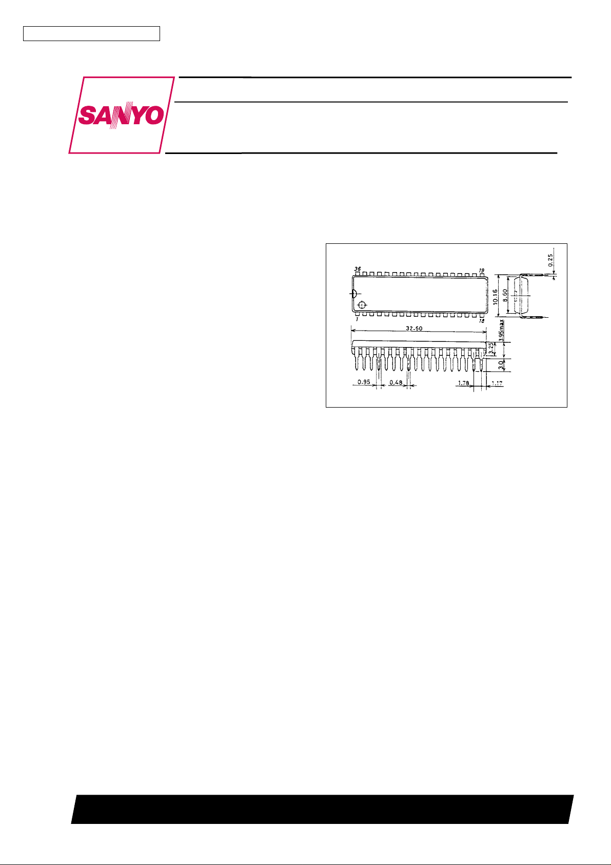
Package Dimensions
unit : mm
3170-DIP36S
[LA7386]
SANYO : DIP36S
Features
.
Includes all functions required for video signal processing in an NTSC VCR.
.
Supports full HQ functions.
YNR on chip (standard).
CNR on chip (external components can be removed for passthrough operation).
Detail enhancer on chip.
Higher white clipping level (190%).
.
In addition to the above, also provides the following functions for excellent image quality:
Edge compensation.
Double high-pass noise canceller → permits wide-band noise reduction.
Linear phase-type image quality adjustment → ideal image quality adjustment method, with no waveform distortion.
.
By adopting the 1CCD method, one comb filter (glass) has become unnecessary.
Has a single 1H-delay CCD and a comb Y/C separation/YNR chroma crosstalk canceller function on chip.
.
Automatic adjustment filter on chip.
Y: LPF
C: 3.58 MHz BPF, 4.21 MHz BPF, LPF (REC)
.
No adjustment required for white and dark clipping levels.
.
Extremely few peripheral components (about 60 components, excluding peripheral components for the CCD).
.
fsc output can be used as clock for OSD IC.
Crystal oscillator for the on-screen display circuit is not required.
.
DCC circuit on chip.
Suppresses flicker at top of screen and reduces AM noise.
.
High-speed AFC circuit.
Prevents color alteration and loss at top of screen when dubbing.
.
Head switching noise reduction circuit on chip.
.
Smallest package in the industry.
.
Few components needed.
SANYO Electric Co.,Ltd. Semiconductor Bussiness Headquarters
TOKYO OFFICE Tokyo Bldg., 1-10, 1 Chome, Ueno, Taito-ku, TOKYO, 110 JAPAN
22896HA(II) No.5472 - 1/13
LA7386
Maximum Ratings at Ta = 25°C
Parameter Symbol Conditions Ratings Unit
Maximum supply voltage V
Allowable power dissipation Pdmax Ta % 65°C 1070 mW
Operating temperature Topr –10 to +65 °C
Storage temperature Tstg –40 to +150 °C
Operating Conditions at Ta = 25°C
Parameter Symbol Conditions Ratings Unit
Recommended supply voltage V
Operating supply voltage range V
Operating Characteristics at Ta = 25°C, VCC=5V
Parameter Symbol Conditions min typ max Unit
[REC Mode Y]
Current consumption REC I
AGC adjustment CAGC V
VCA control characteristics 1 VCA 1 Measure T3 output level when S9 is set to 2 0.48 0.5 0.52 Vp-p
VCA control characteristics 2 VCA 2 Measure T3 output level when S9 is set to 4 0.48 0.5 0.52 Vp-p
AGC adjustment voltage V
AGC detection voltage V
EE output level V
AGC output 1 AGC 1 V
AGC output 2 AGC 2 V
AGC output 3 AGC 3 V
AGC output 4 AGC 4 V
Sync separation output level V
Sync separation output pulse
width
Sync separation output leading
edge delay time
Sync separation threshold level TH
Sync tip level,
pedestal level,
white level measurement
(REC)
VCA detection voltage VVCA Measure T8 DC voltage 2.80 2.95 3.10 V
Comb filter adjustment V
Y-comb characteristics GY-Comb Measure the chroma level at T2 with a spectrum
C-comb characteristics GC-Comb V
R When VCC= 5 V (when there is no signal),
CC
AGC
AD
EE
SYR
PW
SYR
∆ T
SYR
SYR
L
VOR
max 7.0 V
CC
CC
op 4.8 to 5.2 V
CC
5.0 V
95 120 145 mA
measure sum of incoming currents at pins 29 and
24
= 1.0 Vp-p video signal, use VR33 to adjust
IN
T3 output to 0.5 Vp-p
Measure T33 DC voltage in above state 3.2 3.4 3.6 V
Measure T32 DC voltage in same manner 1.2 1.4 1.6 V
Measure T28A output level in same manner 0.95 1.0 1.05 Vp-p
= 2.0 Vp-p video signal
IN
Measure T3 output level
= 0.5 Vp-p video signal
IN
Measure T3 output level
= 714 mVp-p LUMI, 572 mVp-p SYNC,
IN
measure T3 SYNC level
= 714 mVp-p LUMI, 143 mVp-p SYNC,
IN
measure T3 SYNC level
VIN= 1.0 Vp-p video signal,
500 520 540 mVp-p
460 480 500 mVp-p
135 150 165 mVp-p
90 100 110 mVp-p
4.0 4.2 4.4 Vp-p
T26 output pulse peak value
VIN= 1.0 Vp-p video signal,
4.0 4.3 4.6 µs
T26 output pulse width
VIN= 1.0 Vp-p video signal, measure delay time
0.8 1.0 1.2 µs
of output SYNC versus input SYNC
Gradually attenuate the input level, measure input
–18 –14 dB
level at point when output pulse width widens 1
µs or more beyond PWSYR
Measure electric potential for each of the T28
video output sync tip, pedestal, and white peak,
and assign the measured values to L
and L
= off, adjust so that the 3.58 MHz component at
, respectively
WHI
= standard multiburst signal 1 Vp-p and S30
IN
SYN,LPED
,
T21 is at a minimum
–25 dB
analyzer, V
1 Vp-p and S30 = off
= white 50% + CW 3.0 MHz –25 dB
IN
= standard chroma noise test signal
IN
Continued on next page.
No.5472 - 2/13
Continued from preceding page.
Parameter Symbol Conditions min typ max Unit
REC YNR operation
EP/LP (1)
REC YNR operation
EP/LP (2)
Pre-CCD LPF
frequency characteristics (1)
Pre-CCD LPF
frequency characteristics (2)
3MLPF
frequency characteristics (1)
3MLPF
frequency characteristics (2)
3MLPF
frequency characteristics (3)
3MLPF
frequency characteristics (4)
3MLPF
frequency characteristics (5)
FM modulator output level V
FM modulator
secondary distortion
FM modulator
modulation sensitivity
FM modulator linearity L
1/2 f
carrier shift 1 C
H
1/2 f
carrier shift 2 C
H
Emphasis gain G
Detail enhancer characteristics
(1)
Detail enhancer characteristics
(2)
Detail enhancer characteristics
(3)
Detail enhancer characteristics
(4)
Nonlinear emphasis
characteristics (1)
Nonlinear emphasis
characteristics (2)
LA7386
VR-YNR1 Measure the YNR addition level at T2 with V
standard color bar signal 1 Vp-p and S30 = off
VR-YNR2 Measure the YNR addition level at edit mode T2
G
PFIL1
G
PFIL2
G
3MLP1
G
3MLP2
G
3MLP3
G
3MLP4
G
3MLP5
H
S
FM
MOD
MOD
with V
S30=off
Input a standard multiburst signal (1 Vp-p) and
measure the 4 MHz response for 500 kHz at T11
10 MHz response for 500 kHz at T11 when
V
S30=off
1 MHz response for 500 kHz at T2 when VIN=
standard multiburst signal 1 Vp-p and S30 = off
2 MHz response for 500 kHz at T2 when VIN=
standard multiburst signal 1 Vp-p and S30 = off
3 MHz response for 500 kHz at T2 when VIN=
standard multiburst signal 1 Vp-p and S30 = off
3.58 MHz response for 500 kHz at T2 when
V
S30=off
4.2 MHz response for 500 kHz at T2 when
V
S30=off
No input, use VR36 to adjust output frequency to
4 MHz, measure output level
Ratio of 8 MHz component to 4 MHz in the above
state
Measure amplitude of change in output frequency
when 2.6 V DC or 3.1 V DC is applied to T3,
= standard color bar signal 1 Vp-p and
IN
= standard multiburst signal 1 Vp-p and
IN
= standard multiburst signal 1 Vp-p and
IN
= standard multiburst signal 1 Vp-p and
IN
2 x (f3.1 – f2.6)
MOD
S1
S2
Measure output frequency when 2.85 V DC
applied to T3, f2.85
L
f2.85 – (f3.1 + f2.6)/2
=
MOD
f3.1 – f2.6
x 100
Measure amplitude of change in output frequency
when SW35B is from on to off and SW35A is off
Measure amplitude of change in output frequency
when SW35A is on and SW35B is switch from on
to off
EMP
VIN= 0.5 mVp-p 10 kHz sine wave
Measure ratio of levels of input and output
amplitude at T4
G
ENH1
G
ENH2
G
ENH3
G
ENH4
G
NLEMP1VIN
G
NLEMP2VIN
VIN= 158 mVp-p 2 MHz sine wave
Measure ratio of levels of T4 and T3, difference
with G
EMP
VIN= 50 mVp-p 2 MHz sine wave
Measure ratio of levels of T4 and T3, difference
with G
EMP
VIN= 15.8 mVp-p 2 MHz sin wave
Measure ratio of levels of T4 and T3, difference
with G
EMP
VIN= 15.8 mVp-p 2 MHz sine wave
Measure output amplitude at T4 in edit mode,
difference with G
EMP
= 500 mVp-p 2 MHz
Measure ratio of levels of T4 and T3, difference
with G
EMP
= 158 mVp-p 2 MHz
Measure ratio of levels of T4 and T3, difference
with G
EMP
IN
=
10 12 14 mV
234mV
–0.5 0 +0.5 dB
–10 –8 –6 dB
–0.5 0 +0.5 dB
–1 0 +1 dB
–10 –8 –6 dB
–30 dB
–15 dB
0.89 1.0 1.12 Vp-p
–40 –35 dB
1.6 2.0 2.4 MHz/V
–3 0 +2 %
6.8 7.8 9.5 kHz
6.8 7.8 9.5 kHz
–0.5 0 +0.5 dB
1.6 1.9 2.6 dB
3.1 4.1 5.1 dB
5.3 6.3 7.3 dB
2.9 3.9 4.9 dB
0.5 1.4 2.3 dB
2.6 3.8 5.2 dB
Continued on next page.
No.5472 - 3/13

Continued from preceding page.
Parameter Symbol Conditions min typ max Unit
Nonlinear emphasis
characteristics (3)
Main linear emphasis
characteristics (1)
Main linear emphasis
characteristics (2)
Detail enhancer US mode
characteristics (1)
Detail enhancer US mode
characteristics (2)
White clipping level L
Dark clipping level L
[PB Mode Y]
Current consumption PB I
Dropout compensation period T
FM demodulation voltage V
FM demodulation sensitivity S
FM demodulation linearity L
Carrier leakage CL V
Noncorrelation detection level V
PB YNR characteristics
LP/EP (1)
PB YNR characteristics
LP/EP (2)
PB YNR characteristics
SP (3)
Playback through gain G
Dropout detection (feedback)
level
Nonlinear de-emphasis
characteristics (1)
Nonlinear de-emphasis
characteristics (2)
Double noise canceller
characteristics (1)
Double noise canceller
characteristics (2)
G
NLEMP3VIN
G
ME1
G
ME2
G
ENHS1
G
ENHS2
WC
DC
P Incoming currents at pins 29 and 24 when
CC
DOC
DEM4
DEM
DEM
CORR
GP-YNR1 V
GP-YNR2 V
GP-YNR3 V
PB
L
DOC
GNL
DEEM1NIN
GNL
DEEM2
G
WNC1
G
WNC2
LA7386
= 50 mVp-p 2 MHz
Measure ratio of levels of T3 and T4, difference
with G
EMP
VIN= 50 mVp-p 500 kHz sine wave
Measure ratio of levels of T4 and T3, difference
with G
EMP
VIN= 50 mVp-p 2 MHz
Measure ratio of levels of T4 and T3, difference
with G
EMP
Measure the amplitude at T4 when
V
= 15.8 mVp-p 2 MHz sine wave; compare
IN
level with G
EMP
Measure the amplitude at T4 when
V
= 15.8 mVp-p 2 MHz sine wave in edit mode;
IN
compare level with G
EMP
VIN= 500 mVp-p white 100% video
Measure white clipping level at T4
VIN= 500 mVp-p white 100% video
Measure dark clipping level at T4
V
= 5.0 V
CC
T33A: 4 MHz, 300 mVp-p sine wave
T3A: 0.5 Vp-p video signal
T33A: time from when input went to 0 until T28A
output returned
VIN= 300 mVp-p,f=4MHz, output voltage 0.9 1.05 1.15 V
VIN= 300 mVp-p,f=2MHz, V
VIN= 300 mVp-p,f=6MHz, V
Calculate S
L
=
DEM
= 300 mVp-p,f=4MHz
IN
Ratio between 4 MHz component of T1 and
S
DEM
V
DEM
DEM4
V
=(V
DEM2–VDEM6
–(V
DEM2+VDEM6
DEM2–VDEM6
DEM2
DEM6
)/4
)/2
x 100
VIN= 500 mVp-p video signal (ramp waveform) 22 IRE
= 500 mVp-p noise test signal –30 dB
IN
S/N difference with S6 on/off
= 500 mVp-p noise test signal –30 dB
IN
S/N difference with EDIT on/off; pin 36 low
= 500 mVp-p noise test signal, –30 dB
IN
S6 edit on/off S/N ratio Pin36 low
Apply VIN= 0.5 Vp-p video signal to pin 3, and
determine ratio between pin 28 output level and
input level
T33A: 4 MHz, 300 mVp-p sine wave
T3A: 0.5 Vp-p video signal
Measure input signal level when T33A signal
drops momentarily and T28A output goes to 0
= white 50% video + sine wave
f = 2 MHz, 158 mVp-p
Measure I/O response, and assign output level
described above as 0 dB
f = 2 MHz, 50 mVp-p –9.0 –8.0 –7.0 dB
f = 2 MHz, 158 mVp-p –2.3 –1.8 –1.3 dB
f = 2 MHz, 50 mVp-p –6.0 –5.0 –4.0 dB
4.9 6.4 7.9 dB
4.9 5.2 5.5 dB
13.1 13.6 14.1 dB
2.9 3.9 4.9 dB
0.7 1.7 2.7 dB
186 193 200 %
–50 –45 –40 %
125 155 185 mA
0.6 1.0 ms
0.11 0.14 0.17 V/MHz
–3.5 0 +3.5 %
–40 –35 dB
2.5 dB
1.5 dB
1.5 dB
4.5 6.0 7.5 dB
30 40 50 mVp-p
–6.0 –5.0 –4.0 dB
Continued on next page.
No.5472 - 4/13
 Loading...