

SANYO LA7357 Datasheet
Overview
The LA7357 can be used as a PAL/SECAM
discrimination IC. Since no ceramic resonator or tank
circuit is required, only a small number of external
components are used, and the LA7357 can contribute to
reduced mounting areas and lower system costs.
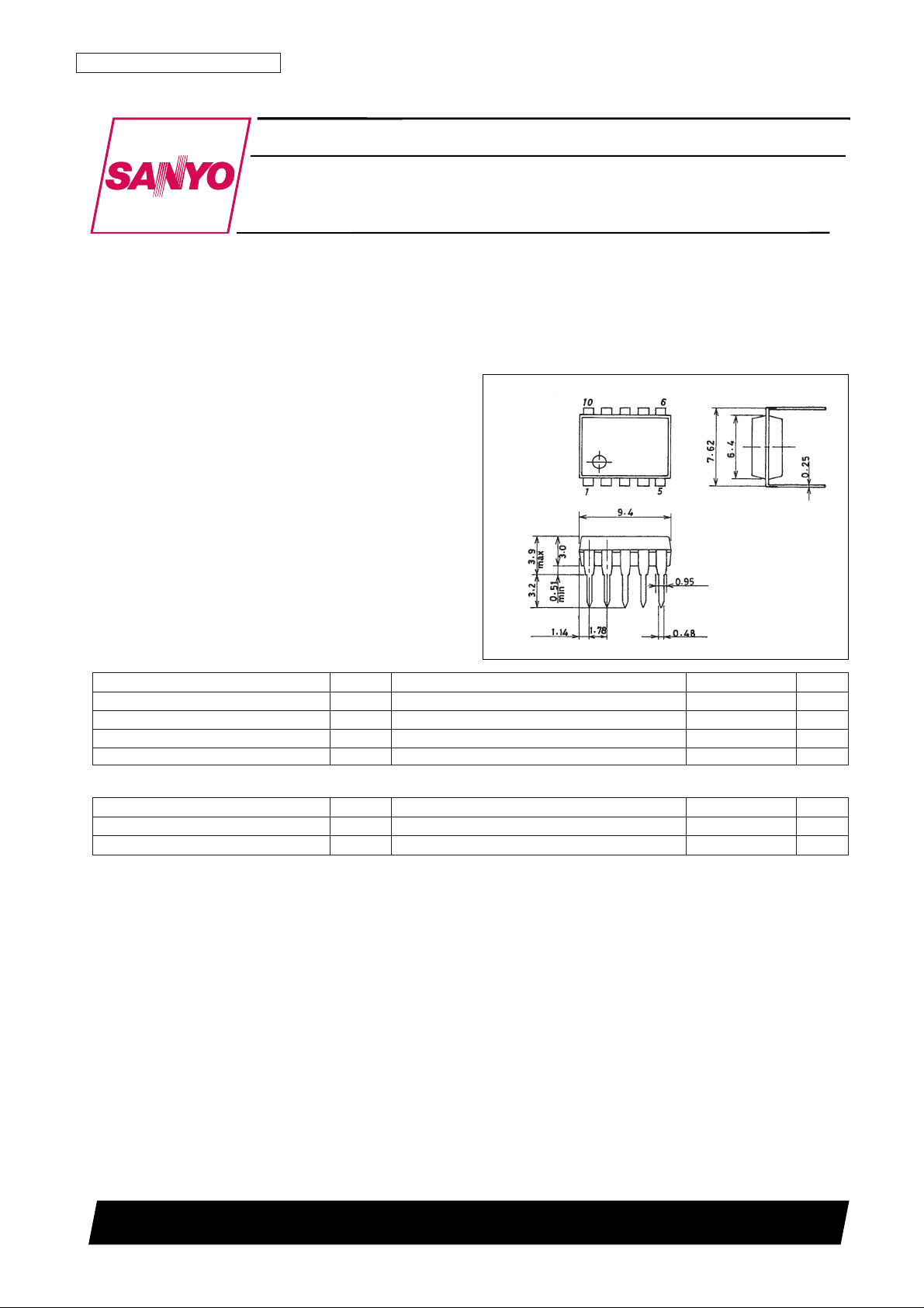
Package Dimension
unit: mm
3098B-DIP10S
Monolithic Linear IC
Ordering number : EN5654
73097HA(OT) No. 5654-1/6
SANYO: DIP10S
[LA7357]
SANYO Electric Co.,Ltd. Semiconductor Bussiness Headquarters
TOKYO OFFICE Tokyo Bldg., 1-10, 1 Chome, Ueno, Taito-ku, TOKYO, 110 JAPAN
PAL/SECAM Discrimination Circuit for VHS VCRs
LA7357
Parameter Symbol Conditions Ratings Unit
Maximum supply voltage V
CC
max 7.0 V
Allowable power dissipation Pd max Ta ≤ 65 °C 120 mW
Operating temperature Topr –10 to +65 °C
Storage temperature Tstg –40 to +125 °C
Parameter Symbol Conditions Ratings Unit
Supply voltage V
CC
5.0 V
Operating voltage range V
CC
op 4.8 to 5.5 V
Operating Conditions at Ta = 25°C
Specifications
Maximum Ratings at Ta = 25°C
No. 5654-2/6
LA7357
Parameter Symbol Conditions
Ratings
Unit
min typ max
Current drain
I
CC
1 Pin 5 = ground, pin 7 influx current: T4 output 7.0 10.0 13.0 mA
I
CC
2 Pin 5 = VCC, pin 7 influx current: T4 output 7.5 10.5 13.5 mA
The pin 5 voltage when the pin 2 output
appears when slowly raising the voltage
BGP threshold level BTH applied to pin 5 from 0 V. 2.2 2.5 2.8 V
The input signal should be 300 mVp-p:
T2 output
The pin 5 voltage when the pin 2 output
appears when slowly lowering the voltage
SYNC threshold level STH applied to pin 5 from 5 V. 0.6 0.8 1.0 V
The input signal should be 300 mVp-p:
T2 output
Stipulated as the output ratio when a
Input limiter amplifier gain LIMG 10 mVp-p amplitude sine wave is input to 9 12 15 dB
pin 1: T2 output
Measure the output amplitude when a
Input limiter amplifier level LIMD 300 mVp-p amplitude sine wave is input to 150 190 230 mVp-p
pin 1: T2 output
The V1 level when T1 switches from low to
Comparator hysteresis high-level voltage Comp H high when slowly raising V1 from 0 V: T1 2.7 3.0 3.3 V
output
The V1 level when T1 switches from high to
Comparator hysteresis low-level voltage Comp L low when slowly lowering V1 from 5 V: T1 2.0 2.3 2.6 V
output
DET-OUT output high-level voltage DETH With a 2-kΩ load: T1 output 3.6 4.0 4.4 V
DET-OUT output low-level voltage DETL With a 2-kΩ load: T1 output 0 0.2 0.4 V
Operating Characteristics at Ta = 25°C, VCC= 5 V
Switching Conditions
Symbol
Input signal Input pulse Applied voltage Switch states
S1 S2 S3 S4 V1 V2 SW1 SW2 SW3 SW4 SW5
I
CC
1 No signal No signal 0 V 0 V Off Off Off Off Off
I
CC
2 No signal No signal 5 V 5 V Off Off Off Off Off
BTH Sig.1 No signal1 0 V 0 V
Variable DC level
On Off On Off Off
STH No signal Sig.1 0 V 0 V
Variable DC level
On Off On Off Off
LIMG Sig.1 No signal 5 V 0 V On Off Off Off Off
LIMD Sig.1 No signal 5 V 0 V On Off Off Off On
Comp H No signal No signal No signal No signal
Variable DC level
Off On Off Off On
Comp L No signal No signal No signal No signal
Variable DC level
Off On Off Off On
DETH Sig.2 Sig.1 P2 P1 Off Off Off Off On
DETL Sig.3 Sig.1 P2 P1 Off Off Off Off On
 Loading...