

SANYO LA7337 Datasheet
Monolithic Linear IC
Ordering number : N5288A
13097 HA (OT) No. 5288-1/7
SANYO Electric Co.,Ltd. Semiconductor Bussiness Headquarters
TOKYO OFFICE Tokyo Bldg., 1-10, 1 Chome, Ueno, Taito-ku, TOKYO, 110 JAPAN
SECAM-Format VCR
Chroma Signal-Processing Circuit
LA7337
Overview
The LA7337 is an IC that implements SECAM-format
VCR signal processing in a single chip. It incorporates
band-pass filters and a SECAM discrimination circuit on
chip and features automatic adjustment of the bell filter for
a reduced number of external components and adjustmentfree circuit operation.
Features
• All required filters, except for the bell filter,
incorporated on chip.
• Automatic adjustment of the bell filter f0parameter
• Built-in SECAM discrimination circuit
Functions
•4.3-MHz and 1.1-MHz band-pass filters, limiter, AGC (in
playback mode)
• Divide-by-four circuit, 4× frequency multiplier circuit,
2.2-MHz band-pass filter
• Bell filter f0automatic adjustment circuit, SECAM
discrimination circuit
• Sync gate
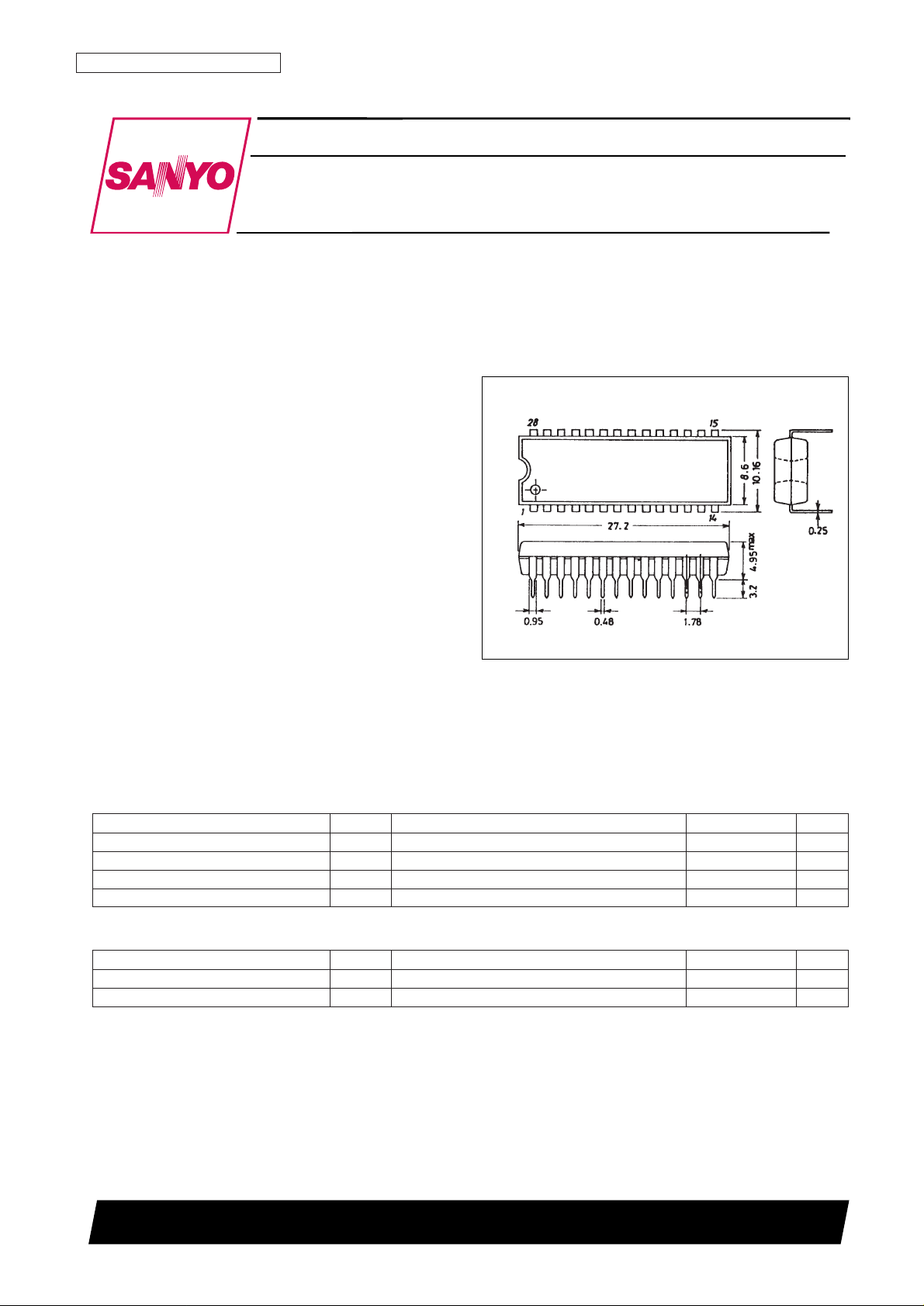
Package Dimensions
unit: mm
3063-DIP28S
SANYO: DIP28S
[LA7337]
Parameter Symbol Conditions Ratings Unit
Maximum supply voltage V
CC
max 7V
Allowable power dissipation Pd max Ta ≤ 70°C 600 mW
Operating temperature Topr –15 to +70 °C
Storage temperature Tstg –40 to +150 °C
Specifications
Absolute Maximum Ratings at Ta = 25°C
Parameter Symbol Conditions Ratings Unit
Recommended supply voltage V
CC
5V
Operating supply voltage range V
CC
op 4.8 to 5.5 V
Operating Conditions at Ta = 25°C
No. 5288-2/7
LA7337
Parameter Symbol Conditions
Ratings
Unit
min typ max
Record mode current drain I
CCR
V5 = V6 = 0 V, V16 = 0 V, S27 = composite
50 70 90 mA
sync., S15 = color bar signal
4.3-MHz band-pass filter characteristics (1) V
F4C
V6 = 5 V, V16 = 0 V, S27 = composite sync.
145 180 215 mVp-p
S15 = sine wave (200 mVp-p, f = 4.286 MHz)
As above, except S15 = sine wave
4.3-MHz band-pass filter characteristics (2) G
F4L1
(200 mVp-p, f = 1.1 MHz), taking V
F4C
as the –30 –20 dB
reference (0 dB)
As above, except S15 = sine wave
4.3-MHz band-pass filter characteristics (3) G
F4L2
(200 mVp-p, f = 2.2 MHz), taking V
F4C
as the –10 –5 dB
reference (0 dB)
As above, except S15 = sine wave
4.3-MHz band-pass filter characteristics (4) G
F4H
(200 mVp-p, f = 7.5 MHz), taking V
F4C
as the –30 –20 dB
reference (0 dB)
V5 = V6 = 0 V, V16 = 0 V, SW21B = on,
Record mode bell filter center frequency (1) F
BLR1
S15 = sine wave (200 mVp-p, f = 4 to 5 MHz), 4.243 4.286 4.329 MHz
S27 = composite sync.
Record mode bell filter center frequency (2) F
BLR2
As above, except V5 = 4 V. 4.493 4.536 4.579 MHz
V5 = V6 = 0 V, V16 = 0 V, SW21B = on,
Record mode bell filter characteristics (1) V
BLRC
S15 = sine wave (200 mVp-p, f = FBLR1), 200 250 300 mVp-p
S27 = composite sync.
As above, except S15 = sine wave
Record mode bell filter characteristics (2) G
BLRL
(200 mVp-p, f = 3.8 MHz), taking V
BLRC
as –14 –11 –8 dB
the reference (0 dB)
As above, except S15 = sine wave
Record mode bell filter characteristics (3) G
BLRH
(200 mVp-p, f = 4.8 MHz), taking V
BLRC
as –14 –11 –8 dB
the reference (0 dB)
V5 = V6 = 0 V, S15 = a SECAM color bar
Record mode killer operating level G
KLR
signal (variable level), V16 = 0 V, SW21B = on,
–28 –23 –18 dB
V23 = 3.4 V, V24 = 3.7 V, S27 = composite sync.
SW1 = on, V1 = 5 V, V5 = V6 = 0 V, V16 = 0 V,
Record equalization center frequency (1) F
EQR1
S21 = sine wave (200 mVp-p, f = 4 to 5 MHz),
1.0608 1.0715 1.0822 MHz
SW21A = SW21B = on, S27 = composite sync.
Record equalization center frequency (2) F
EQR2
As above, except V6 = 4 V 1.0788 1.0895 1.1002 MHz
SW1 = on, V1 = 5 V, V5 = V6 = 0 V, V16 = 0 V,
Record equalization characteristics (1) V
EQRC
S21 = sine wave (200 mVp-p, f = FEQR1 × 4),
65 85 105 mVp-p
SW21A = SW21B = on, S27 = composite sync.
Record equalization characteristics (2) G
EQRL
As above, except S21 = sine wave (200 mVp-p,
8 11 14 dB
f = 3.8 MHz), taking V
EQRC
as the reference (0 dB)
Record equalization characteristics (3) G
EQRH
As above, except S21 = sine wave (200 mVp-p,
8 11 14 dB
f = 4.8 MHz), taking V
EQRC
as the reference (0 dB)
SW1 = on, V1 = 5 V, V5 = V6 = 0 V, V16 = 0 V,
Record chrominance signal output level V
OR
S15 = sine wave (200 mVp-p, f = 4.4 MHz), 80 110 140 mVp-p
SW21B = on, S27 = composite sync.
Record chrominance signal output unnecessary
As above, except measure the 2.2 MHz
spectrum (1)
GSR1 component in the T11 signal. Taking V
OR
as –30 –20 dB
the reference (0 dB).
Record chrominance signal output unnecessary
As above, except measure the 3.3 MHz
spectrum (2)
GSR2 component in the T11 signal. Taking V
OR
as –30 –20 dB
the reference (0 dB).
V5 = V6 = 0 V, V16 = 5 V, S27 = composite
Playback mode current drain I
CCP
sync., S13 = sine wave 60 80 100 mA
(50 mVp-p, f = 1.0715 MHz)
V6 = 5 V, SW8B = on, V16 = 5 V,
AGC control characteristics (1) V
AGC
S27 = composite sync., S13 = sine wave 90 120 150 mVp-p
(50 mVp-p, f = 1.0715 MHz)
As above, except S13 = sine wave
AGC control characteristics (2) G
AGC1
(100 mVp-p, f = 1.0715 MHz) –1 0 +1 dB
Taking V
AGC
as the reference (0 dB).
As above, except S13 = sine wave
AGC control characteristics (3) G
AGC2
(25 mVp-p, f = 1.0715 MHz) –1 0 +1 dB
Taking V
AGC
as the reference (0 dB).
V6 = 5 V, SW14 = on, V14 = V14R,
1.1-MHz band-pass filter characteristics (1) G
F1L
S13 = sine wave (50 mVp-p, f = 500 kHz),
–3 0 +3 dB
V16 = 5 V, S27 = composite sync., taking
VAGC as the reference (0 dB).
As above, except S13 = sine wave
1.1-MHz band-pass filter characteristics (2) G
F1H1
(50 mVp-p, f = 2.2 MHz) –30 –20 dB
Taking V
AGC
as the reference (0 dB).
As above, except S13 = sine wave
1.1-MHz band-pass filter characteristics (3) G
F1H2
(50 mVp-p, f = 3.3 MHz) –35 –25 dB
Taking V
AGC
as the reference (0 dB).
Operating Characteristics at Ta = 25°C, VCC= 5 V
Continued on next page.
No. 5288-3/7
LA7337
Continued from preceding page.
Parameter Symbol Conditions
Ratings
Unit
min typ max
V6 = 0 V, SW8B = on, SW14 = on,
Playback equalization center frequency (1) F
EQP1
V14 = V14R, S13 = sine wave
1.0608 1.0715 1.0822 MHz
(50 mVp-p, f = 1 to 1.2 MHz), V16 = 5 V,
S27 = composite sync.
Playback equalization center frequency (2) F
EQP2
As above, except V6 = 4 V 1.0788 1.0895 1.1002 MHz
V6 = 0 V, SW8B = on, SW14 = on,
Playback equalization characteristics (1) V
EQPC
V14 = V14R, S13 = sine wave
120 150 180 mVp-p
(50 mVp-p, f = FEQP1), V16 = 5 V,
S27 = composite sync.
As above, except S13 = sine wave
Playback equalization characteristics (2) G
EQPL
(50 mVp-p, f = 950 kHz), taking V
EQP
as the –14 –11 –8 dB
reference (0 dB).
As above, except S13 = sine wave
Playback equalization characteristics (3) G
EQPH
(50 mVp-p, f = 1.2 MHz), taking V
EQP
as the –14 –11 –8 dB
reference (0 dB).
SW1 = on, V1 = 5 V, V5 = V6 = 0 V,
Playback bell center frequency (1) F
BLP1
SW8A = SW8B = on, V16 = 5 V,
4.243 4.286 4.329 MHz
S27 = composite sync., S8 = sine wave
(200 mVp-p, f = 1 to 1.2 MHz),
Playback bell center frequency (2) F
BLP2
As above, except V5 = 4 V 4.493 4.536 4.579 MHz
SW1 = on, V1 = 5 V, V5 = V6 = 0 V,
Playback bell characteristics (1) V
BLPC
SW8A = SW8B = on, S8 = sine wave
65 85 105 mVp-p
(200 mVp-p, f = FBLP × 1/4), V16 = 5 V,
S27 = composite sync.
As above, except S8 = sine wave
Playback bell characteristics (2) G
BLPL
(200 mVp-p, f = 950 kHz), taking V
BLPC
as 8 11 14 dB
the reference (0 dB).
As above, except S8 = sine wave
Playback bell characteristics (3) G
BLPH
(200 mVp-p, f = 1.2 MHz), taking V
BLPC
as 8 11 14 dB
the reference (0 dB).
SW1 = on, V1 = 5 V, V5 = V6 = 0 V, V16 = 5 V,
Playback chrominance signal output level V
OP
S13 = sine wave (200 mVp-p, f = 1.1 MHz), 130 160 190 mVp-p
SW8B = on, S27 = composite sync.
Playback chrominance signal output
As above, except measure the 2.2 MHz
unnecessary spectrum (1)
GSP1 component in the T17 signal. Taking V
OP
as –25 –15 dB
the reference (0 dB).
Playback chrominance signal output
As above, except measure the 3.3 MHz
unnecessary spectrum (2)
GSP2 component in the T17 signal. Taking V
OP
as –20 –10 dB
the reference (0 dB).
CLK input level V
CLK
f = 4.433619 MHz 100 200 800 mVp-p
Synchronizing signal input threshold level V
THS
1.8 2 2.2 V
SW1 = on, V1 = 5 V, V5 = V6 = 0 V, V16 = 0 V,
Record mode sync gate start time (muting off) T
RGB
S15 = sine wave (200 mVp-p, f = 4.286 MHz), –0.3 +0.2 +0.7 µs
SW21B = on, S27 = composite sync.
Record mode sync gate start time (muting on) T
RGBM
As above, except SW2 = on 1.5 2 2.5 µs
Record mode sync gate release time T
RGE
As above 4.5 5.0 5.5 µs
Record mode mute setting resistance VTSP2 10 20 30 kΩ
SW1 = on, V5 = V6 = 0 V, SW8B = on,
Playback mode sync gate start time T
PGB
S13 = sine wave (50 mVp-p, f = 1.0715 MHz), 1.5 2 2.5 µs
V16 = 5 V, S27 = composite sync.
Playback mode sync gate release time T
PGE
As above 4.5 5.0 5.5 µs
BGP start time T
BGB
V5 = 0 V, V6 = 5 V, SW21B = on, V16 = 0 V,
6.0 6.5 7.0 µs
S27 = composite sync.
BGP amplitude T
BGW
As above 2.0 2.5 3.0 µs
SECAM discriminator output resistance R26 SW25 = on, V25 = 5 V 7 10 13 kΩ
Record mode SECAM discriminator
V5 = V6 = 0 V, V16 = 0 V, SW21B = on,
characteristics (1)
V
SCMR1
S27 = composite sync., S15 = SECAM color 4.5 V
bar signal
Record mode SECAM discriminator
V
SCMR2
As above, except S15 = PAL color bar signal 0.5 V
characteristics (2)
Continued on next page.
 Loading...