

SANYO LA7289 Datasheet
Parameter Symbol Conditions Ratings Unit
Maximum supply voltage V
CC
max 14 V
Pin 2 input voltage V
IN
2DC ±45 Vp-p
Pin 2 input current I
IN
2 ±1.5 mA
Allowable power dissipation Pd max Ta ≤ 65 °C 500 mW
Operating temperature Topr –10 to +65 °C
Storage temperature Tstg –55 to +150 °C
Ordering number : EN5642
43097HA(OT) No. 5642-1/11
Overview
The LA7289 includes on chip all functions required for
the record and playback of VCR audio signals and
achieves complete adjustment-free operation by the
adoption of an automatic record bias current adjustment
circuit. In addition, the inclusion of a switching circuit for
switching between tuner and line input in addition to the
circuits provided by earlier ICs makes the LA7289 truly
optimal for audio VCR products.
Functions
• Equalizer amplifier
• Ripple filter
• Record/playback switching circuit
• Muting
• SP/LP/EP switching circuit
• Record amplifier
• ALC
• Tape head switching circuit
• Automatic record bias adjustment circuit
• Input switching circuit (line/tuner)
Features
• Adjustment-free record bias current (automatic
adjustment circuit adopted)
• Built-in record bias oscillator circuit power supply
switch
• Record equalizer choke coil no longer required
• Playback amplifier input noise voltage: 1.0 µV rms
• Value of the ALC detector capacitor reduced (to 3.3 µF)
• Built-in high-voltage head switching circuit
• Supply voltage: supports both 9 and 12-V operation
• Built-in input switching circuit (for the line and tuner
inputs)
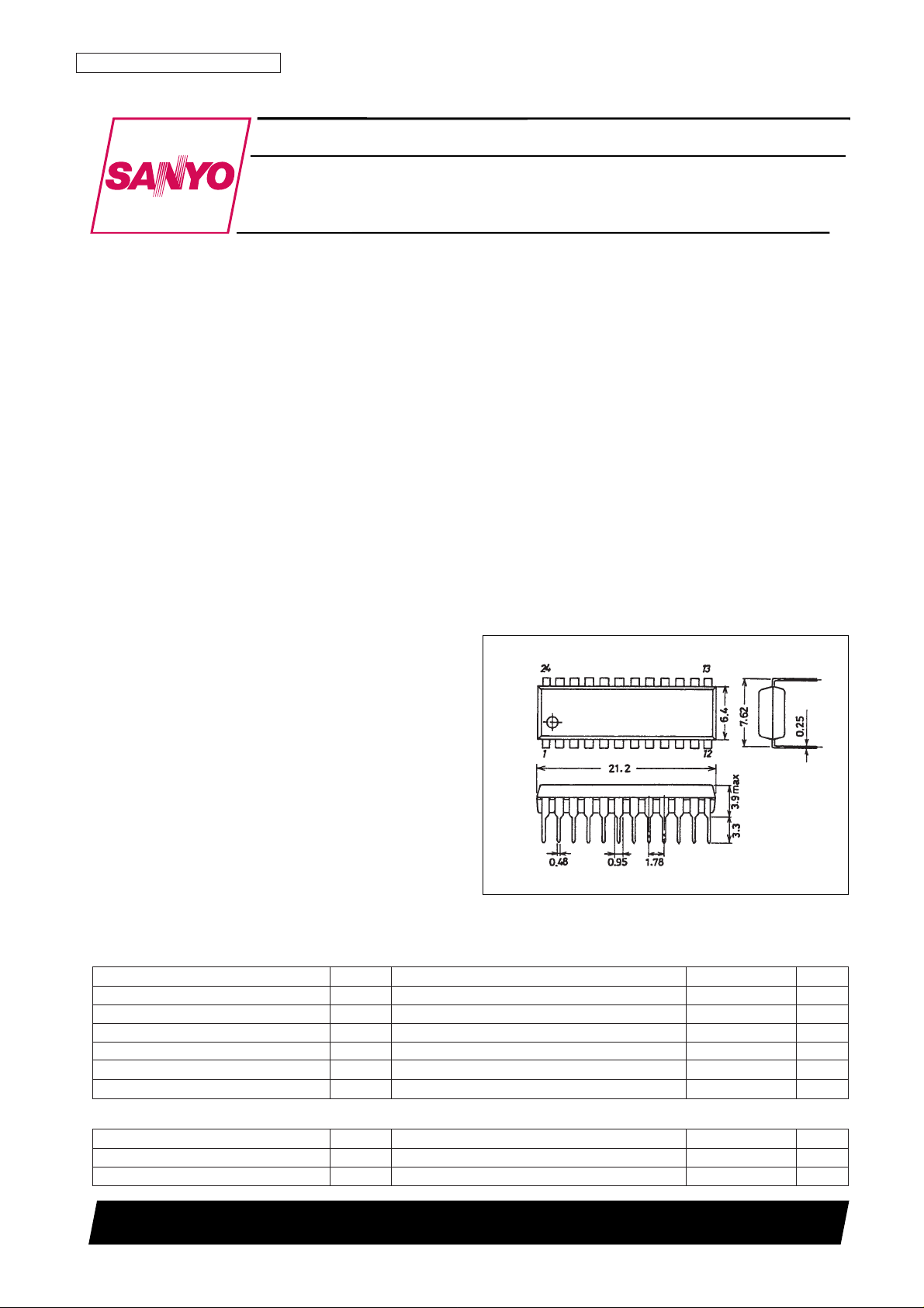
Package Dimensions
unit: mm
3067-DIP24S
SANYO: DIP24S
[LA7289]
LA7289
SANYO Electric Co.,Ltd. Semiconductor Bussiness Headquarters
TOKYO OFFICE Tokyo Bldg., 1-10, 1 Chome, Ueno, Taito-ku, TOKYO, 110 JAPAN
VCR Audio Signal Record and Playback Processor
Monolithic Linear IC
Specifications
Maximum Ratings at Ta = 25°C
Parameter Symbol Conditions Ratings Unit
Recommended supply voltage V
CC
9, 12 V
Allowable operating voltage range V
CC
op 8.5 to 12.5 V
Operating Conditions at Ta = 25°C
No. 5642-2/11
LA7289
Parameter Symbol Conditions
Ratings
Unit
min typ max
Current drain (EE) I
CCE
No signal 10.0 12.5 15.0 mA
Current drain (playback) I
CCP
No signal 11.2 14.0 16.8 mA
Current drain (record) I
CCR
No signal 9.6 12.0 14.4 mA
[Equalizer amplifier]
Open-circuit voltage gain VG
OE
VO= –6dBV 58.4 64.4 – dB
Input noise voltage V
NIE
Rg = 620 Ω, DIN audio filter – 1.0 1.8 µVrms
[Line Amplifier]
Voltage gain (PB input) VG
LP
VO= –6dBV 20.1 20.6 21.1 dB
Voltage gain (LINE input) VG
LL
VO= –6dBV 20.1 20.6 21.1 dB
Voltage gain (TUNER input) VG
LT
VO= –6dBV 20.1 20.6 21.1 dB
Harmonic distortion THD
L
VO= –6dBV – 0.05 0.3 %
Output noise voltage V
NOL
Rg = 620 Ω, DIN audio filter – –75 –69 dBV
Maximum output voltage V
OML
THD = 1% 1.7 2.5 – Vrms
Output voltage when ALC operating V
OA
VIN= –25dBV –7 –6 –5 dBV
ALC effect ALC V
IN
= –25dBV to –5dBV – 1 3 dB
Total harmonic distortion when ALC operating
THD
A
VIN= –25dBV – 0.05 0.6 %
[Record Amplifier]
Voltage gain VG
CR
VO= –6dBV 13.5 14.0 14.5 dB
Harmonic distortion THD
R
VO= –6dBV – 0.05 0.3 %
Maximum output voltage V
OMR
THD = 1% 1.7 2.5 – Vrms
[REC/EE Switching Circuit]
Record mode hold voltage V
RR
The pin 19 DC voltage 3.6 – 6.0 V
EE mode hold voltage V
RE
The pin 19 DC voltage 0 – 1 V
[Muting Circuit]
On state hold voltage V
MON
The pin 18 DC voltage 3.6 – 6.0 V
Off state hold voltage V
MOFF
The pin 18 DC voltage 0 – 1 V
Muting attenuation
M
P
, ML, M
T
80 90 – dB
(PB, LINE. TUNER)
[PB, LINE. TUNER Switching Circuit]
PB mode hold voltage V
LP
The pin 17 DC voltage 3.6 – 6.0 V
LINE mode hold voltage V
LL
The pin 17 DC voltage 1.8 – 2.6 V
TUNER mode hold voltage V
LT
The pin 17 DC voltage 0 – 1.0 V
[EP. LP. SP Switching Circuit]
EP mode hold voltage V
EE
The pin 16 DC voltage 3.6 – 6.0 V
LP mode hold voltage V
EL
The pin 16 DC voltage 1.8 – 2.6 V
SP mode hold voltage V
EE
The pin 16 DC voltage 0 – 0.8 V
[Switching Circuit]
Pin 2 on resistance R
ON
2 I1 = ±1 mA – 10 30 Ω
Pin 2 input voltage V
IN
2 Ta = 65°C, f = 70 kHz (sin), ILK= 10 µA – – ±45 V
[Record Bias Automatic Adjustment Circuit]
Record bias current I
B
220 245 270 µA
Pin 1 output control range V1 2.0 4.0 6.0 V
Electrical Characteristics at Ta = 25°C, VCC= 12 V, f = 1 kHz, 0 dBV = 1.0 Vrms
No. 5642-3/11
LA7289
Test Circuit
No. 5642-4/11
LA7289
Switching Operations
Test item (signal) SW1 SW2 SW3 SW4 SW5 SW6 V
M
V
P
V
R
Input Measurement
I
CCE
2 1 3 2 2 2 GND GND GND - I
O
I
CCP
2 1 3 2 2 2 GND 5 V GND - I
O
I
CCR
2 1 3 2 2 2 GND GND 5 V - I
O
VG
OE
1 2 3 2 2 2 GND 5 V GND VIN1 VO1
V
NIE
2 1 3 2 2 2 GND 5 V GND - VO1
VG
LP
, THDL, V
OML
2 1 2 2 2 2 GND 5 V GND VIN2 VO2
VG
LL
2 1 3 2 2 1 GND 2 V GND VIN4 VO2
VG
LT
2 1 3 2 1 2 GND GND GND VIN3 VO2
V
NOL
2 1 3 2 2 2 GND GND GND - VO2
V
OA
, ALC, THD
A
2 1 3 1 1 2 GND GND GND VIN3 VO2
VG
CR
, THDR, V
OMR
2 1 3 2 2 2 GND GND 5 V VIN5 VO3
M
P
1 1 1 2 2 2 5 V 5 V GND VIN1 VO2
M
L
2 1 3 2 2 1 5 V 2 V GND VIN4 VO2
M
T
2 1 3 2 1 2 5 V GND GND VIN3 VO2
I
B
2 1 1 2 2 2 GND GND 5 V - VO4
V1 2 1 1 2 2 2 GND GND 5 V - V1
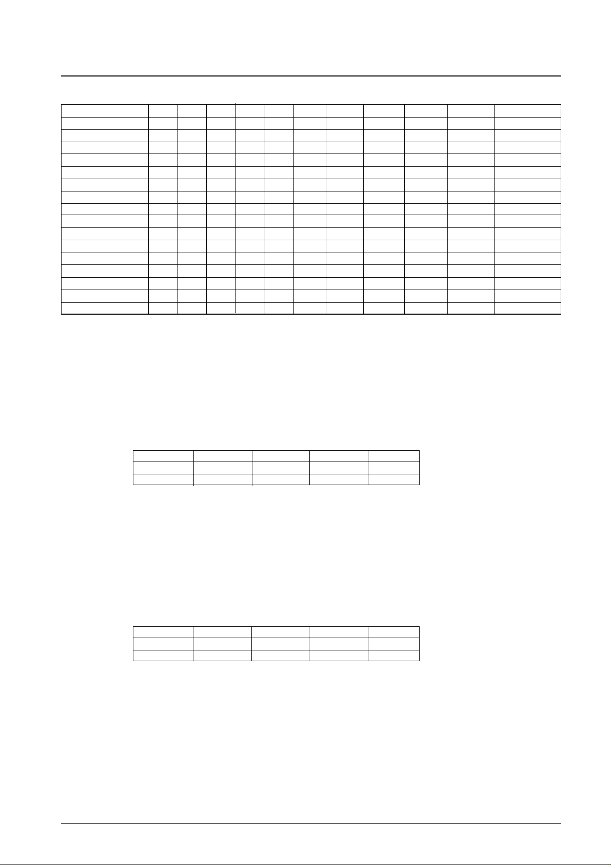
Head Coil Specifications
1. Application circuit 1 (Series erase head type)
• R/P Head 58 kΩ ± 15 % (f = 70 kHz)
• AE Head 34 Ω ± 20 % (f = 70 kHz)
• FE Head 80 Ω ± 15 % (f = 70 kHz)
• Oscillator coil test number: 15419A, Model no. 7QM3
2 Application circuit 2 (Parallel erase head type)
• R/P Head 58 kΩ ± 15 % (f = 70 kHz)
• AE Head 180 Ω ± 20 % (f = 70 kHz)
• FE Head 80 Ω ± 15 % (f = 70 kHz)
• Oscillator coil test number: 15415A, Model no. 7QM3
For more information contact: Tokyo Parts Industries Co., Ltd.
Telephone: +81-270-25-1191
Pin No. 3 - 2 2 - 1 6 - 5 5 - 4
Line type 2UEW-0.09 2UEW-0.09 2UEW-0.09 2UEW-0.09
Total windings 32T 20T 176T 29T
Pin No. 3 - 2 2 - 1 4 - 5 5 - 6
Line type 2UEW-0.10 2UEW-0.10 2UEW-0.10 2UEW-0.10
Total windings 10T 22T 104T 22T
 Loading...