

Page 1
Ordering number: EN 4750
Monolithic Linear IC
LA7286
VCR Audio Signal Recording
and Playback Processor
Functions
.
Equalizer amplifier
.
Line amplifier
.
Recording amplifier
.
Recording bias current automatic adjustment circuit
.
Ripple filter
.
Mute
.
ALC
.
Recording/playback switch
.
SP, LP, EP switch
.
Tape head switch
Features
.
No adjustment of recording bias current required
(due to adoption of automatic adjustment circuit).
.
Recording bias oscillation circuit power supply switch on
chip.
.
Eliminates need for choke coil for recording equalizer.
.
Playback amplifier equivalent input noise voltage:
1.0 µVrms.
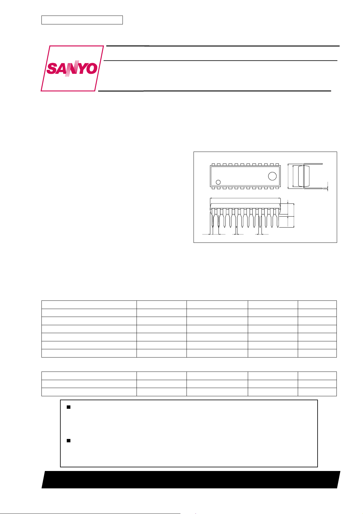
Package Dimensions
unit : mm
3067-DIP24S
0.48
21.2
[LA7286]
0.95
13
6.4
7.62
12
3.25
3.9max
3.3
0.51min
SANYO : DIP24S
24
1
0.81 1.78
.
Reduced capacitance (3.3 µF) of ALC detection capacitor.
.
High withstand voltage head switch on chip.
.
Supply voltage: 9 V and 12 V operation.
Specifications
Maximum Ratings atTa=25°C
Parameter Symbol Conditions Ratings Unit
Maximum supply voltage V
Pin 2 input voltages V
Pin 2 input current I
Allowable power dissipation Pdmax Ta % 65°C 500 mW
Operating temperature Topr –10 to +65
Storage temperature Tstg –55 to +150
max 14 V
CC
2 DC ±65 Vp-p
IN
2 ±1.5 mA
IN
0.25
C
°
C
°
Operating Conditions atTa=25°C
Parameter Symbol Conditions Ratings Unit
Recommended supply voltage V
Operating supply voltage range V
Any and all SANYO products described or contained herein do not have specifications that can handle
applications that require extremely high levels of reliability, such as life-support systems, aircraft’s
control systems, or other applications whose failure can be reasonably expected to result in serious
physical and/or material damage. Consult with your SANYO representative nearest you before using
any SANYO products described or contained herein in such applications.
SANYO assumes no responsibility for equipment failures that result from using products at values that
exceed, even momentarily, rated values (such as maximum ratings, operating condition ranges, or other
parameters) listed in products specifications of any and all SANYO products described or contained
herein.
SANYO Electric Co.,Ltd. Semiconductor Company
TOKYO OFFICE Tokyo Bldg., 1-10, 1 Chome, Ueno, Taito-ku, TOKYO, 110-8534 JAPAN
CC
op 8.5 to 12.5 V
CC
9, 12 V
51595TH (II) No.4750-1/10
Page 2
LA7286
Operating Characteristics atTa=25°C, VCC=12V,f=1kHz, 0 dBV : 1.0 Vrms
Parameter Symbol Conditions min typ max Unit
Current consumption (EE) I
Current consumption (PB) I
Current consumption (REC) I
[Equalizer amplifier]
Open-circuit voltage gain VG
Equivalent input noise voltage V
[Line amplifier]
Voltage gain (PB input) VG
Voltage gain (LINE input) VG
Total harmonic distortion THD
Output noise voltage V
Maximum output voltage V
Output voltage when ALC is on V
ALC effect ALC V
Distortion when ALC is on THD
[Recording amplifier ]
Voltage gain VG
Total harmonic distortion THD
Maximum output voltage V
[Mute circuit]
On voltage V
Off voltage V
Mute attenuation (PB, EE) M
[EP, LP, SP switch circuit]
EP mode hold voltage V
LP mode hold voltage V
SP mode hold voltage V
[EE, PB switch circuit]
EE mode hold voltage V
PB mode hold voltage V
[REC, EE switch circuit]
REC mode hold voltage V
EE mode hold voltage V
[Switch]
Pin 2 on resistance R
Pin 2 input voltage V
[Recording bias current automatic adjustment circuit]
Recording bias current I
Pin 1 output control range V
CCE
CCP
CCR
NIE
NOL
OML
OA
OMR
MON
MOFF
P,ME
EE
EL
ES
LL
LP
RR
RE
ON
IN
B
CTL
No signal 9.5 12.0 14.5 mA
No signal 8.5 11.0 13.5 mA
No signal 8.5 10.5 12.5 mA
VO= –6 dBV 58.4 64.4 dB
OE
Rg = 620 Ω, DIN Audio filter 1.0 1.8 µVrms
VO= –6 dBV 21.0 21.5 22.0 dB
LP
VO= –6 dBV 21.0 21.5 22.0 dB
LR
VO= –6 dBV 0.05 0.3 %
L
Rg=1kΩ, DIN Audio filter –80.0 –74.0 dBV
THD = 1% 1.7 2.5 Vrms
VIN= –26 dBV –7.0 –6.0 –5.0 dBV
= –26 dBV to –6 dBV 1 3 dB
IN
VIN= –26 dBV 0.05 0.6 %
A
VO= –6 dBV 13.5 14.0 14.5 dB
CR
VO= –6 dBV 0.05 0.3 %
R
THD = 1% 1.7 2.5 Vrms
Pin 22 DC voltage 2.5 6.0 V
Pin 22 DC voltage 0 1.5 V
80 90 dB
Pin 21 DC voltage 3.6 6.0 V
Pin 21 DC voltage 1.8 2.6 V
Pin 21 DC voltage 0 1 V
Pin 23 DC voltage 3 6 V
Pin 23 DC voltage 0 1 V
Pin 24 DC voltage 3 6 V
Pin 24 DC voltage 0 1 V
2 I2=±1mA 10 25 Ω
2 Ta=65°C,f=80kHz(sin), ILK=10µA ±45 V
The conditions for using each head assume the
specifications shown below.
220 245 270 µA
2.5 4.0 6.0 V
Head Coil Specifications
(1) Application circuit 1 (erase head series type)
.
R/P Head 58 kΩ (typ) +15% (f = 70kHz)
.
AE Head 34 Ω (typ) +25% (f = 70kHz)
.
FE Head 80 Ω (typ) +20% (f = 70kHz)
.
OSC Coil: Model name 7QM3, Prototype No. C-14290, Tokyo Parts Ind. Co., Ltd. Tel = 0270-25-1191
PinNo. 3to2 2to1 6to5 5to4
Wire type 2UEW 0.09 ←←←
Total number of
coils
–15%
–25%
–10%
32T 20T 180T 25T
No.4750-2/10
Page 3
LA7286
(2) Application circuit 2 (erase head parallel type)
.
R/P Head 58 kΩ (typ) +10% (f = 70kHz)
.
AE Head 180 Ω (typ) +25% (f = 70kHz)
.
FE Head 80 Ω (typ) +20% (f = 70kHz)
.
OSC Coil:Model name 7QM3, Prototype No. C-14284, Tokyo Parts Ind. Co., Ltd.
PinNo. 3to2 2to1 4to5 5to6
Wire type 2UEW 0.10 ←←←
Total number of
coils
* The head specifications are as agreed upon by Alps Electric and Sanyo.
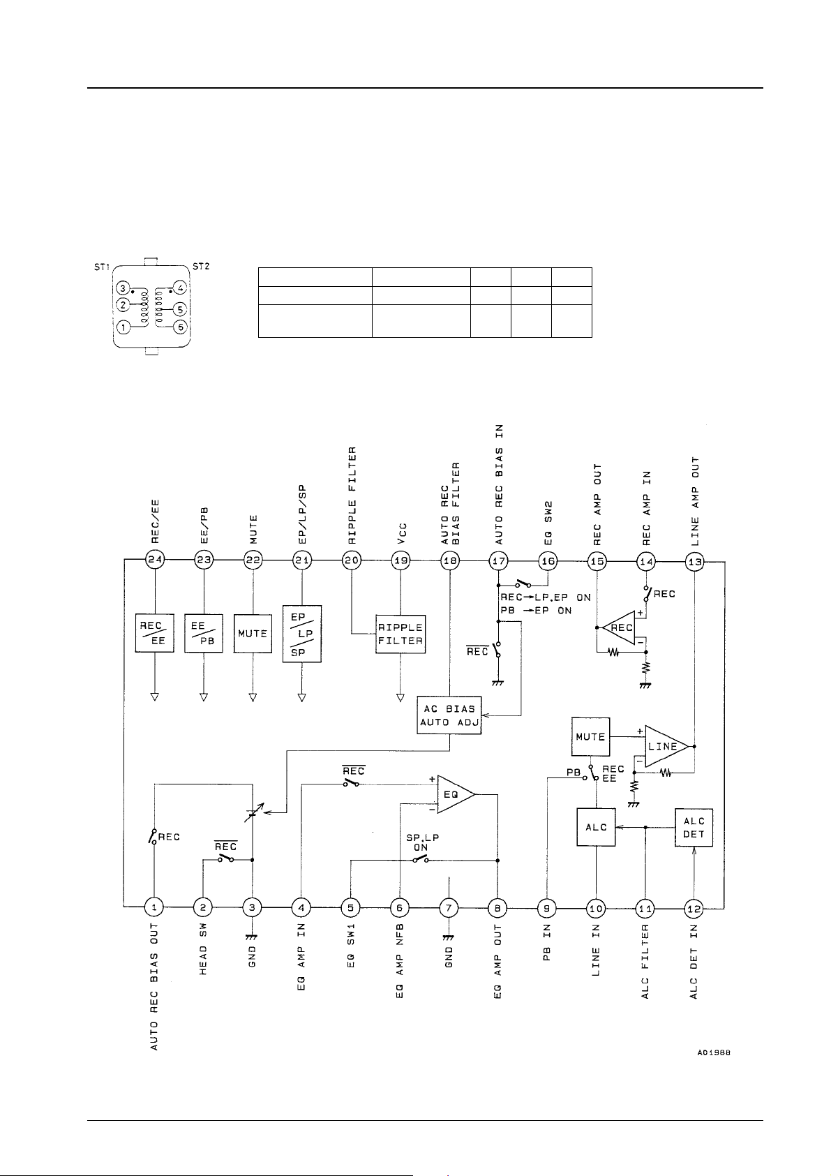
Block Diagram
–20%
–5%
–20%
15T 25T 110T 30T
No.4750-3/10
Page 4

LA7286
Test Circuit
Unit (resistance: Ω, capacitance: F)
Switch Operation Table
Test item (symbol) SW1 SW2 SW3 SW4 SW5 SW6 V
I
CCE
I
CCP
I
CCR
VG
OE
V
INE
VG
, THDL,V
LP
VG
LR
V
ONL
V
, ALC, THD
OA
VG
, THDR,V
R
M
P
M
E
V
BIAS
V
CTL
MOL
A
MOR
213221GND5VGND—I
213221GNDGNDGND—I
213221GND5V5V—I
123221GNDGNDGNDV
213221GNDGNDGND—V
212221GNDGNDGNDV
213121GND5VGNDV
213221GND5VGND—V
213111GND5VGNDV
213221GND5V5VV
1112215VGNDGNDV
2131215V5VGNDV
213222GND5V5V—V
213222GND5V5V—V1
M
V
P
V
Input
R
Measure:
1V
IN
2V
IN
3V
IN
3V
IN
4V
IN
1V
IN
3V
IN
O
O
O
1
O
1
O
2
O
2
O
2
O
2
O
3
O
2
O
2
O
4
O
No.4750-4/10
Page 5

LA7286
Sample Application Circuit : Erase head series type
Unit (resistance: Ω, capacitance: F)
* R3:27kΩ(VCC= 12 V), 4.7 kΩ (VCC=9V)
* TR1 : 2SC3331
Sample Application Circuit : Erase head parallel type
Unit (resistance: Ω, capacitance: F)
* R3:22kΩ(VCC= 12 V), 4.7 kΩ (VCC=9V)
* TR1 : 2SC3331
No.4750-5/10
Page 6

LA7286
Pin Functions
Unit (resistance: Ω)
Pin No. Function name Internal circuit for pin Description of function
1
2
3 GND
4 EQ AMP input
Recording bias
automatic control
output
Head switch
(high withstand
voltage)
EE, PB → off
REC → control voltage
EE, PB → on
REC → off
On resistance →10 Ω (typ)
Withstand voltage when off → ±45 V
(f = 80 kHz)
GND for pin 2 head switch and
Equalizer Amplifier only
Input impedance for playback signal
input from head → 120 kΩ (typ)
5 EQ switch 1
6 EQ AMP NFB
7 GND
Switches the Playback Equalizer
Amplifier high-region frequency
voltage gain.
LP, SP → on
EP → off
On resistance → 20 Ω (typ)
Equalizer Amplifier negative
feedback pin
GND for all circuit blocks except the
pin 2 head switch and Equalizer
Amplifier
Continued on next page.
No.4750-6/10
Page 7

LA7286
Continued from preceding page.
Pin No. Function name Internal circuit for pin Description of function
8 EQ AMP output
9 LINE AMP PB input
Unit (resistance: Ω)
Output impedance → 50Ω (typ)
Inputs the playback signal from the
Equalizer Amplifier. Because the
input impedance is as high as 120
kΩ, a 0.1 µF ceramic capacitor can
be used for the coupling capacitor
on pin 9.
Inputs EE and REC signals.
10 LINE AMP LINE input
11 ALC FILTER
12
ALC input wave
detection
The reference input is set by
resistors R1 and R2. The amplifier
gain is fixed at 21.5 dB. In addition,
because the input impedance is as
high as 120 kΩ, a 0.1 µF ceramic
capacitor can be used for the
coupling capacitor on pin 10.
Wave detection is performed when
connected to GND through a
capacitor. In addition, the attack and
recovery time is set by the C and R
time constants.
Inputs the Line Amplifier output
signal. The ALC level is set by the
resistors R1 and R2.
Continued on next page.
No.4750-7/10
Page 8

LA7286
Continued from preceding page.
Pin No. Function name Internal circuit for pin Description of function
13 LINE AMP output
14 REC AMP input
Unit (resistance: Ω)
Output inpedance → 50 Ω (typ)
Inputs the recording signal from Line
Amplifier.
The recording current is set by the
resistors R1 and R2. In addition,
because the input impedance is as
high as 120 kΩ, a 0.1 µF ceramic
capacitor can be used for the
coupling capacitor on pin 14.
15 REC AMP output
16 EQ switch 2
17
Recording bias
automatic control
input and PB switch.
Output impedance → 50 Ω (typ)
Switches the high-region peaking
frequency during recording and
playback.
REC PB
EP On On
LP On Off
SP Off Off
On resistance → 30 Ω (typ)
EE, PB → on
REC → off
On resistance → 20 Ω (typ)
Continued on next page.
No.4750-8/10
Page 9

LA7286
Continued from preceding page.
Pin No. Function name Internal circuit for pin Description of function
18
19 Supply voltage (V
20 Ripple filter
21 EP/LP/SP Control
Recording bias
automatic control filter
CC
)
Unit (resistance: Ω)
Power supply
of each
circuit block
Wave detection is performed when
connected to GND through a
capacitor.
max=14V
V
CC
V
= 8.5 V to 12.5 V
CC
Ripple rejection is performed when
connected to GND through an
electrolytic capacitor for the filter.
When the voltage on
pin 21 is 3.6 V to 6.0 V: EP;
when 1.8 V to 2.6 V: LP;
when0Vto1.0V:SP
Switch On Pin Number
REC PB
EP 16 16
LP 16, 5 5
SP 5 5
22 MUTE Control
23 EE/PB Control
24 REC/EE Control
When the voltage on
pin 22 is 2.5 V to 6.0 V: MUTE on;
when0Vto1.5V:MUTE off
When the voltage on
pin 23 is 3.0 V to 6.0 V: EE;
when0Vto1.0V:PB
When the voltage on
pin 24 is 3.0 V to 6.0 V: REC;
when 0V to 1.0 V: EE
However, REC mode is entered only
when the voltage on pin 23 is 3.0 V
to 6.0 V.
No.4750-9/10
Page 10

LA7286
f Response f Response
Response — dB
Frequency,f—Hz
Specifications of any and all SANYO products described or contained herein stipulate the performance,
characteristics, and functions of the described products in the independent state, and are not guarantees
of the performance, characteristics, and functions of the described products as mounted in the customer’s
products or equipment. To verify symptoms and states that cannot be evaluated in an independent device,
the customer should always evaluate and test devices mounted in the customer’s products or equipment.
SANYO Electric Co., Ltd. strives to supply high-quality high-reliability products. However, any and all
semiconductor products fail with some probability. It is possible that these probabilistic failures could
give rise to accidents or events that could endanger human lives, that could give rise to smoke or fire,
or that could cause damage to other property. When designing equipment, adopt safety measures so
that these kinds of accidents or events cannot occur. Such measures include but are not limited to protective
circuits and error prevention circuits for safe design, redundant design, and structural design.
In the event that any or all SANYO products(including technical data,services) described or
contained herein are controlled under any of applicable local export control laws and regulations,
such products must not be exported without obtaining the export license from the authorities
concerned in accordance with the above law.
No part of this publication may be reproduced or transmitted in any form or by any means, electronic or
mechanical, including photocopying and recording, or any information storage or retrieval system,
or otherwise, without the prior written permission of SANYO Electric Co. , Ltd.
Any and all information described or contained herein are subject to change without notice due to
product/technology improvement, etc. When designing equipment, refer to the “Delivery Specification”
for the SANYO product that you intend to use.
Information (including circuit diagrams and circuit parameters) herein is for example only ; it is not
guaranteed for volume production. SANYO believes information herein is accurate and reliable, but
no guarantees are made or implied regarding its use or any infringements of intellectual property rights
or other rights of third parties.
Response — dB
Frequency,f—Hz
This catalog provides information as of May, 1995. Specifications and information herein are subject to
change without notice.
PS No.4750-10/10
 Loading...