

Page 1
Ordering number:ENN4040
Monolithic Linear IC
LA7282, 7282M
VCR Audio Signal Recording /
Playback Processor
Overview
The LA7282 and 7282M are small package ICs containing
all functions necessary to record and playback VCR audio
signal.
Features
• Small package leaves large space for other components.
• Delete of In and Output electrolysis capacitor.
• Low capacitor (0.1µF) for the line amplifier inputs (PB
IN and AUDIO IN)
• Non-Adjustment of PB Gain by less gain scatter.
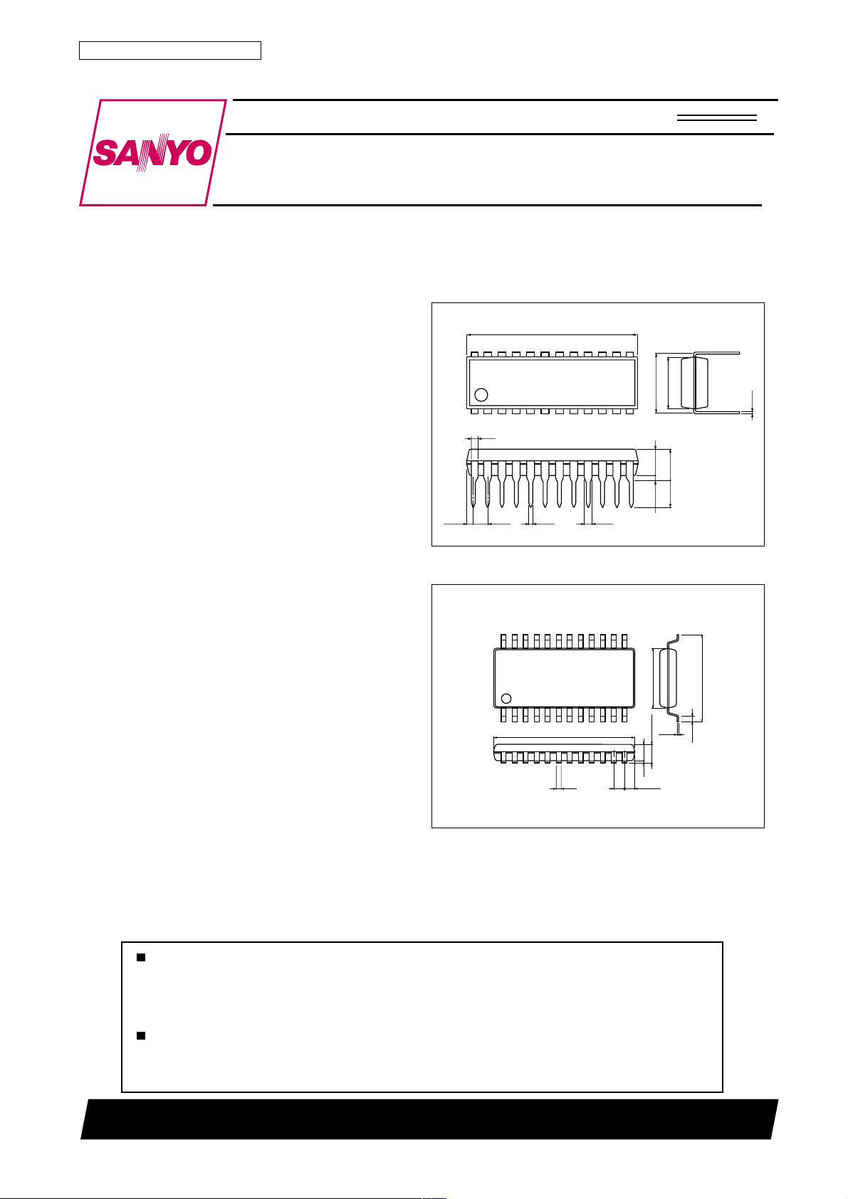
Package Dimensions
unit:mm
3067A-DIP24S
[LA7282]
21.0
24
1
0.9
(0.71)
1.78
unit:mm
3112A-MFP24S
0.48
24
0.95
[LA7282M]
13
6.4
7.62
0.25
12
(3.25)
3.9max
3.3
0.51min
SANYO : DIP24S
13
5.4
112
Any and all SANYO products described or contained herein do not have specifications that can handle
applications that require extremely high levels of reliability, such as life-support systems, aircraft’s
control systems, or other applications whose failure can be reasonably expected to result in serious
physical and/or material damage. Consult with your SANYO representative nearest you before using
any SANYO products described or contained herein in such applications.
SANYO assumes no responsibility for equipment failures that result from using products at values that
exceed, even momentarily, rated values (such as maximum ratings, operating condition ranges,or other
parameters) listed in products specifications of any and all SANYO products described or contained
herein.
12.5
0.35
1.0
0.15
1.7max
0.63
1.5
0.1
(0.75)
SANYO : MFP24S
7.6
SANYO Electric Co.,Ltd. Semiconductor Company
TOKYO OFFICE Tokyo Bldg., 1-10, 1 Chome, Ueno, Taito-ku, TOKYO, 110-8534 JAPAN
O2500TN (KT)/6292TS No.4040–1/7
Page 2
LA7282, 7282M
Specifications
Maximum Ratings at Ta = 25˚C
retemaraPlobmySsnoitidnoCsgnitaRtinU
egatlovylppusmumuxaMV
egatlovtupni1niPV
tnerructupni1niPI
noitapissidrewopelbawollAxamdP 004Wm
erutarepmetgnitarepOrpoT 56+ot01–
erutarepmetegarotSgtsT 521+ot55–
Operating Conditions at Ta = 25˚C
retemaraPlobmySsnoitidnoCsgnitaRtinU
egatlovylppusdednemmoceRV
egnaregatlovgnitarepOV
Operating Characteristics at Ta = 25˚C, VCC=12V, f=1kHz, 0dBv= : 1.0Vrms
retemaraPlobmySsnoitidnoC
)EF(niardtnerruCI
)BP(niardtnerruCI
)CER(niardtnerruCI
edomBPtaniagllarevOGV
]reifilpmagnizilauqE[
niagegatlovpoolnepOGV
egatlovesiontupnitnelaviuqEV
ecnadepmitupnIZ
]reifilpmaeniL[
)NIBP(niagegatloVGV
)NICER,EE(niagegatloVGV
noitrotsidcinomrahlatoTDHT
egatlovesiontuptuOV
)NIBP(ecnadepmitupnIZ
)NICER,EE(ecnadepmitupnIZ
egatlovtuptuomumixaMV
CLAtaegatlovtuptuOV
tceffECLACLAV
CLAtanoitrotsidcinomrahlatoTDHT
]reifilpmagnidroceR[
)poolnepo(niagegatloVGV
)pooldesolc(niagegatloVGV
noitrotsidcinomrahlatoTDHT
ecnadepmitupnIZ
egatlovtuptuomumixaMZ
]tiucricgnituM[
egatlovnOV
egatlovffOV
)EE,BP(levelnoitaunettaetuMM
)CER(levelnoitaunettaetuMM
]tiucricrotcelesEE/BP[
egatlovdlohedomBPV
egatlovdlohedomEEEPVCD,32niP3.30.6V
]tiucricrotcelesEE/CER[
egatlovdlohedomCERV
egatlovdlohedomEEV
]tiucricrotcelesrezilauqE[
egatlovnohctiwSV
egatlovffohctiwSV
]hctiwsrotcelesdaeH[
ecnatsiserno1niPR
ecnatsiserno2niPR
egatlovtupni1niPV
xam 41V
CC
Ta=65˚C, f=80kHz (sin), ILK=10µA
1NI
1NI
Ta≤65˚C, when mounted on the recommended PCB
CC
po 57.21ot52.11V
CC
ECC
PCC
RCC
BP
EO
EIN
ENI
PL
RL
LVO
LON
1NI
2NI
LMO
AO
A
RO
RC
RVO
RNI
RMO
NOM
FFOM
PM,E
R
PP
RR
ER
NOE
FFOE
1NO
2NO
Ta=65˚C, f=80kHz (sin), ILK=10µA
1NI
tnecseiuQ0.80.210.71Am
tnecseiuQ0.90.310.81Am
tnecseiuQ0.70.010.41Am
V,TUOENIL-NIQE
V
V
V
V
V
V
V
vBd5–=0.660.17Bd
O
Ω retlifoiduaNID,2.18.1smrVµ
k2.2=gR
vBd5–=0.125.120.22Bd
O
vBd5–=0.125.120.22Bd
O
vBd5–=3.05.0%
retlifoiduaNID0.07– 0.46– vBd
%3=DHT5.11.2smrV
vBd82–=0.9– 0.8– 0.7– vBd
NI
NI
NI
O
O
%3=DHT5.10.2smrV
vBd8–ot82–=5.10.3Bd
vBd82–=52.06.0%
vBd5–=0.740.25Bd
vBd5–=5.210.315.31Bd
vBd5–=1.03.0%
CD,22niP8.30.6V
CD,22niP00.1V
CD,32niP00.1V
CD,42niP3.3V
CD,42niP00.1V
CD,12,02niP5.30.6V
CD,12,02niP08.0V
Am1±=1I5103
Am1±=2I501
vBd5–=0.955.950.06Bd
O
5.1±Am
0.21V
sgnitaR
nimpytxam
031kΩ
021kΩ
021kΩ
05kΩ
0.080.09Bd
0.560.07Bd
CC
54±V
)54±(09p-pV
˚C
˚C
tinU
V
Ω
Ω
No.4040–2/7
Page 3
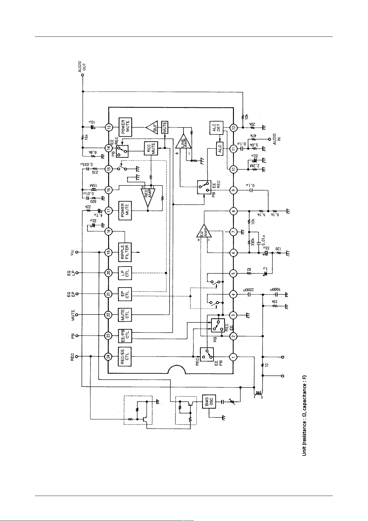
Block Diagram
LA7282, 7282M
No.4040–3/7
Page 4

Test Circuit
LA7282, 7282M
<Switch Setting Table>
)lobmyS(retemaraP1WS2WS3WS4WS5WSVMV
I
ECC
I
PCC
RCCI 21121 DNGV5V5 – A
GV
BP
GV
EO
V
EIN
GV
DHT,
PL
LV,LMO
GV
RL
V
LON
V
AO
GV
GV
RC
M
P
M
R
M
E
DHT,CLA,
A
RO
V,RDHT,
RMO
21121 DNGV5DNG – A
21121 DNGDNGDNG – A
11121 DNGDNGDNGV
12221 DNGDNGDNGV
21221 DNGDNGDNG – VO1
21221 DNGDNGDNGV
21121 DNGV5DNGV
21221 DNGV5DNG – VO2
21211 DNGV5DNGV
21222 DNGV5DNGV
21221 DNGV5DNGV
11121 V5DNGDNGV
21121 V5V5DNGV
21221 V5V5DNGV
V
P
R
tupnItnemerusaeM
1V
NI
1V
NI
2V
NI
3V
NI
3V
NI
4V
NI
4V
NI
1V
NI
4V
NI
2V
NI
Pin Assignment
2
O
1
O
2
O
2
O
2
O
3
O
3
O
2
O
3
O
2
O
No.4040–4/7
Page 5

LA7282, 7282M
Pin Functions
.oNniPnoitcnuFtiucriClanimreT noitpircseD
11hctiwSdaeH
)egatlovhgiH(
2tupnIPMAQE
dna
2hctiwSdaeH
3DNG .hctiwsPEkcabyalpdnaPMAQE,1hctiwsdaeh1niprofDNGevisulcxenA
41hctiwSPE .ycneuqerftnanoserdaehepatehtsteS
52hctiwSPE kcabdeefevitagengnicuderybseicneuqerfrehgihtaniagegatlovehtsesaercnI
6BFNPMAQE gnizilauqederisedhsilbatseotPMAQEehtfokcabdeefevitagenfotupnI
7DNG .1hctiwsdaehdnaPMAQEroftpecxestiucricllarofnruternommoC
8tuptuOPMAQE
Unit (resistance : Ω)
.scitsiretcarahc
ffo:CER;no:BP,EE
01:ecnatsisernO Ω .epyt,
)zHk08=f(V54±:ffognirudegatlovdnatshtiW
.daehehtotlangiskcabyalptupnI
k031:ecnadepmitupnI Ω .pyt,
ffo:BP;no:CER,EE
5:ecnatsisernohctiwS Ω .pyt,
51:ecnatsisernO Ω .pyt
k021:ecnadepmitupnI Ω )edomPEkcabyalp(.pyt,
.PMAQEBPehtfotnuoma
51:ecnatsisernO Ω .pyt,
k21:ecnadepmitupnI Ω )edomPEkcabyalp(.pyt,
9BPPMAENIL
01RETLIFCLA emitCRehT.noitcetedselbaneroticapacahguorhtDNGotnipsihtgnitcennoC
11oiduAPMAENIL
21tupnItceteDCLA
31tuptuOPMAENIL 05:ecnadepmituptuO Ω .pyt,
tupnI
.langisCER,EEtupnI
tupnI
.Fµ1.0foroticapac
.Fµ1.0foroticapacgnilpuocllamsaseriuqerdna
.emityrevocerkcattastestnatsnoc
Select value of R1 and R2 so that the reference input
is at the shoulder of the ALC.
.Bd5.12roftesebdluohsniagreifilpmaehT
k021(hgihsi11nipfoecnadepmitupniehT Ω gnilpuocllamsaseriuqerdna)
Accepts the output signal of LINE amplifier.
The ALC level is determined by the voltage divider
consisting of R
and R2.
1
k021(hgihsi9nipfoecnadepmitupniehT.PMAQEehtotlangisBPtupnI Ω)
41tupnIPMACER .PMAENILmorflangisgnidrocertupnI
Input current is set by the divider consisting of R1 and
R2.
Pin 14 requires no coupling capacitor since REC AMP
is to operate at zero level and as inverting amplifier.
Continued on next page.
No.4040–5/7
Page 6

LA7282, 7282M
Continued from preceding page. Unit (resistance : Ω)
.oNniPnoitcnuFtiucriClanimreT noitpircseD
51hctiwSPL .PLrofelbatiusycneuqerfehtottniopgnikaephgihehtsteS
61BFNPMACER .esirotycneuqerfgnikaepasesuacnipsihtotkrowtenR,C,LnagnitcennoC
71tuptuOPMACER 04:ecnadepmituptuO Ω .pyt
81retliFelppiR .selppirsehtoomsDNGdnanipsihtssorcaroticapaccitylortceleagnitcennoC
51:ecnatsisernO Ω .pyt
k06:ecnadepmitupnI Ω .pyt
91egatloVylppuS
V(CC)
02lortnoCPL .)51nip(hctiwsPLnosnrutnipsihtot)xamV0.6(eromroCDV5.3gniylppA
12lortnoCPE )5,4nip(hctiwsPEnosnrutnipsihtot).xamV0.6(eromroCDV5.3gniylppA
22lortnoCETUM ehT.tiucricetumnosnrutnipsihtot).xamV0.6(eromroCDV8.3gniylppA
32lortnoCBP roV0.1dnaedomEEsretnenipsihtot).xamV0.6(eromroCDV3.3gniylppA
V
CC
V
CC
xamV51=
]edomlortnoC[
edoM
edoMBP
edoMEE
.pytV57.21-52.11=
.wolebroV8.0taffosnruthctiwsehT
.wolebroV0.1tadelbasedsietum
]L[ETUM]H[ETUM
PMAENILPMACERPMAENILPMACER
°
°
edoMCER
°
[ : Pass signal, × : Block signal]
×××
°
°°
.wolebroV8.0taffonrutsehctiwsehT.)51nip(hctiwsPLdna
××
×
°
.edomBPwoleb
42lortnoCCER V0.1dnaedomCERsretnenipsihtot)CCVotpu(eromroCDV0.3gniylppA
.edomEEwolebro
No.4040–6/7
Page 7

LA7282, 7282M
Specifications of any and all SANYO products described or contained herein stipulate the performance,
characteristics, and functions of the described products in the independent state, and are not guarantees
of the performance, characteristics, and functions of the described products as mounted in the customer's
products or equipment. To verify symptoms and states that cannot be evaluated in an independent device,
the customer should always evaluate and test devices mounted in the customer's products or equipment.
SANYO Electric Co., Ltd. strives to supply high-quality high-reliability products. However, any and all
semiconductor products fail with some probability. It is possible that these probabilistic failures could
give rise to accidents or events that could endanger human lives, that could give rise to smoke or fire,
or that could cause damage to other property. When designing equipment, adopt safety measures so
that these kinds of accidents or events cannot occur. Such measures include but are not limited to protective
circuits and error prevention circuits for safe design, redundant design, and structural design.
In the event that any or all SANYO products(including technical data,services) described or
contained herein are controlled under any of applicable local export control laws and regulations,
such products must not be exported without obtaining the export license from the authorities
concerned in accordance with the above law.
No part of this publication may be reproduced or transmitted in any form or by any means, electronic or
mechanical, including photocopying and recording, or any information storage or retrieval system,
or otherwise, without the prior written permission of SANYO Electric Co. , Ltd.
Any and all information described or contained herein are subject to change without notice due to
product/technology improvement, etc. When designing equipment, refer to the "Delivery Specification"
for the SANYO product that you intend to use.
Information (including circuit diagrams and circuit parameters) herein is for example only ; it is not
guaranteed for volume production. SANYO believes information herein is accurate and reliable, but
no guarantees are made or implied regarding its use or any infringements of intellectual property rights
or other rights of third parties.
This catalog provides information as of October, 2000. Specifications and information herein are subject
to change without notice.
PS No.4040–7/7
 Loading...