

Page 1

Ordering number : EN4850A
93098HA (OT) / 30895TH (OT) No. 4850-1/24
LA7265W
SANYO Electric Co.,Ltd. Semiconductor Bussiness Headquarters
TOKYO OFFICE Tokyo Bldg., 1-10, 1 Chome, Ueno, Taito-ku, TOKYO, 110-8534 JAPAN
Single-Chip Black and White CCD Camera
Signal Processing IC
Monolithic Linear IC
Any and all SANYO products described or contained herein do not have specifications that can handle
applications that require extremely high levels of reliability, such as life-support systems, aircraft’s
control systems, or other applications whose failure can be reasonably expected to result in serious
physical and/or material damage. Consult with your SANYO representative nearest you before using
any SANYO products described or contained herein in such applications.
SANYO assumes no responsibility for equipment failures that result from using products at values that
exceed, even momentarily, rated values (such as maximum ratings, operating condition ranges, or other
parameters) listed in products specifications of any and all SANYO products described or contained
herein.
Overview
The LA7265W is a single-chip IC that provides the signal
processing required by black and white CCD cameras.
This IC is optimal for surveillance cameras, door intercom
cameras, and personal computer input cameras due to its
ultraminiature package, low current drain, wide dynamic
range, and high AGC gain.
Functions
• CCD clamping
• CDS (built-in S/H capacitor)
• IRIS amplifier
• AGC backlight correction
• S-curve gamma correction
• Aperture correction
• Variable setup
• Sync addition
• CCD clipping
• IRIS window
• AGC amplifier
• Gamma correction (0.45, 1.0 and variable)
• 1H interpolation switch
• Aperture low illumination suppression
• Variable W.C.
• 75 Ω drivers
Features
• CCD clamping used to provide a wide dynamic range:
The LA7265W can handle a 1.5 Vp-p CCD signal data
level.
• Reduced sampling noise provided by a built-in CDS
capacitor.
• Variable AGC gain: up to a maximum of 32 dB.
• Backlight correction provided by weighting the iris and
AGC levels.
• Three different gamma correction circuits, including Scurve gamma correction
• Knee characteristics are added to the gamma correction
to prevent incorrect white rendering in low light
situations.
• Automatic aperture adjustment according to the
brightness
• Reduced current drain (under 40 mA)
• Ultraminiature package (SQFP48)
• Reduced external component count (50% as compared
to the earlier Sanyo LA7261M)
• Reduced number of adjustment points (two points)
Page 2
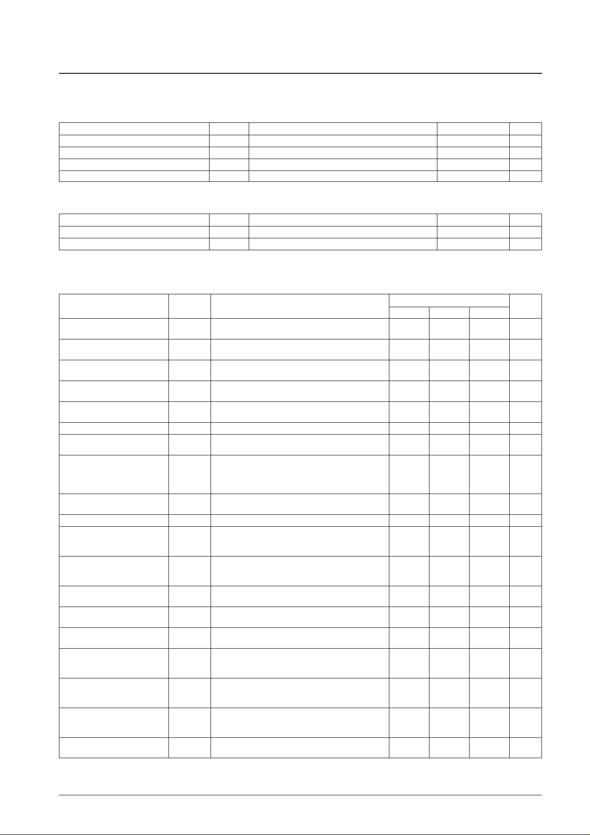
Specifications
Maximum Ratings at Ta = 25°C
Recommended Operating Conditions at Ta = 25°C
Note: Full IC immersion solder dip mounting techniques should be avoided.
Operating Characteristics at Ta = 25°C, VCC= 5 V
No. 4850-2/24
LA7265W
Parameter Symbol Conditions Ratings Unit
Maximum supply voltage V
CC
max 6.0 V
Allowable power dissipation Pd max Ta ≤ 65°C 270 mW
Operating temperature Topr –15 to +65 °C
Storage temperature Tstg –40 to +150 °C
Parameter Symbol Conditions Ratings Unit
Recommended supply voltage V
CC
5.00 V
Operating supply voltage range V
CC
op 4.75 to 5.25 V
Parameter Symbol Conditions
Ratings
Unit
min typ max
CCD clipping high level CCLIPH
Measure the output voltage difference for inputs of
1.11 1.22 1.33 V
0 Vp-p and 2 Vp-p. T1 output
CCD clipping middle level CCLIPM
Measure the output voltage difference for inputs of
0.60 0.91 1.22 V
0 Vp-p and 2 Vp-p. T1 output
CCD clipping low level CCLIPL
Measure the output voltage difference for inputs of
0.25 0.40 0.50 V
0 Vp-p and 2 Vp-p. T1 output
CDS dynamic range CDSD
Measure the output amplitude for a 2 Vp-p input.
1.20 1.47 V
T4 output
CDS hold ability CDSH
Measure the voltage drop during a 30/fsc hold
58 88 mV
for a 1 Vp-p input. T1 output
CDS offset CDSO Measure the output noise level. T1 output 11 mV
Sampling noise CDSN
Stipulated as the absorption remainder for the input
4 mV
dark current difference (200 mV). T1 output
Measure the output voltage for a 500 mVp-p input and
CDS linearity CDSL
the output voltage for a 1000 mVp-p input. Stipulates
100 %
the voltage difference of those two measurements
as a gain ratio. T1 output
IRIS.OUT DC level IRISDC
Measure the output voltage (OPB) with no input.
0.78 1.10 1.42 V
T2 output
IRIS.OUT pedestal level IRISP Measure the pedestal level with no input. T2 output –20 +300 +620 mV
Measure the output voltage for a 300 mVp-p input.
IRIS.OUT maximum W.C. level IRISWL Stipulated as the difference between that measurement –490 –230 +30 mV
and the IRISDC level. T2 output
Measure the output voltage difference for inputs of
IRIS.OUT gain IRISG 0 Vp-p and 300 mVp-p. Stipulated as the gain with 7.5 9.0 10.5 dB
respect to the input. T2 output
IRIS.OUT D range IRISD
Measure the output voltage difference for inputs of
2.05 2.40 V
0 Vp-p and 2 Vp-p. T2 output
IRIS.OUT W.C. level initial value IRISWT
Measure the output voltage difference for inputs of
1.25 1.60 1.95 V
0 Vp-p and 2 Vp-p. T2 output
AGC DC level (maximum) AGCDC1
Measure the output voltage (OPB) with no input.
0.85 2.10 3.50 V
T1 output
Measure the output voltage difference for inputs of
AGC maximum gain (maximum) AGCHG1 0 Vp-p and 30 mVp-p. Stipulated as the gain with 26.0 31.0 34.5 dB
respect to the input. T1 output
Measure the output voltage difference for inputs of
AGC maximum gain (typical) AGCHG2 0 Vp-p and 30 mVp-p. Stipulated as the gain with 19.5 24.0 27.5 dB
respect to the input. T1 output
Measure the output voltage difference for inputs of
AGC maximum gain (minimum) AGCHG3 0 Vp-p and 30 mVp-p. Stipulated as the gain with 13.5 15.5 17.5 dB
respect to the input. T1 output
AGC DC level (minimum) AGCDC2
Measure the output voltage (OPB) with no input.
2.30 2.50 2.70 V
T1 output
Continued on next page.
Page 3
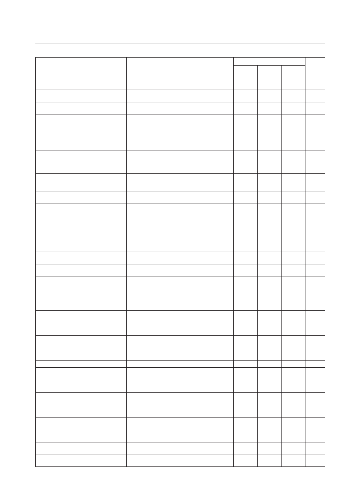
Continued from preceding page.
No. 4850-3/24
LA7265W
Parameter Symbol Conditions
Ratings
Unit
min typ max
Measure the output voltage difference for inputs of
AGC minimum gain AGCLG 0 Vp-p and 300 mVp-p. Stipulated as the gain with –3.5 –2.0 –0.5 dB
respect to the input. T1 output
AGC minimum D range AGCLD
Measure the output voltage difference for inputs of
0.63 1.80 V
0 Vp-p and 300 mVp-p. T1 output
AGC W.C. level AGCWC
Measure the WC voltage for a 300 mVp-p input.
3.83 4.15 4.47 V
T1 output
Measure the output voltage difference for inputs of
AGC standard voltage AGCT
0 Vp-p and 100 mVp-p by adjusting VR4. Stipulated
2.07 2.13 2.19 V
as the VR4 voltage when that difference is 400 mVp-p.
T1 output
AGC frequency characteristics AGCF
Stipulated as the gain difference between f = 10 MHz
–6.0 –5.0 dB
and f = 500 kHz. T1 output
Measure the output voltage difference for inputs of
AGC linearity AGCL
0 mVp-p and 25 mVp-p and the output voltage difference
95 %
for inputs of 100 mVp-p and 125 mVp-p. Stipulated as
the ratio of those two gains. T1 output
Increase the lower side input pulse voltage and
Y1.IN clamping input low level CLP2L measure the input pulse level when the clamping level 1.26 1.40 V
begins to change. T9 output
AGC detector DC level DETDC
Measure the output voltage (OPB) with no input.
2.28 2.38 2.48 V
T3 output
AGC detector pedestal level DETP
Measure the pedestal level with no input.
58 70 82 mV
T3 output
Measure the output voltage for a 300 mVp-p input.
AGC detector maximum W.C. level DETWL Stipulated as the difference between that measurement –150 –110 –70 mV
and the detector DC level. T3 output
Measure the output voltage difference for inputs of
AGC detector gain DETG 0 Vp-p and 300 mVp-p. Stipulated as the gain with 8.4 8.8 9.2 dB
respect to the input. T3 output
AGC detector D range DETD
Measure the output voltage difference for inputs of
1.21 1.33 V
0 Vp-p and 1500 mVp-p. T3 output
AGC detector W.C. level
DETWT
Measure the output voltage difference for inputs of
0.70 0.90 1.10 V
initial value 0 Vp-p and 1500 mVp-p. T3 output
AGC control characteristics 1 CONT1 Measure the output DC voltage. T4 output 0.92 1.12 1.22 V
AGC control characteristics 2 CONT2 Measure the output DC voltage. T4 output 0.92 2.00 3.10 V
AGC control characteristics 3 CONT3 Measure the output DC voltage. T4 output 2.90 3.00 3.10 V
γ = 0.45 DC level γ1DC
Measure the output voltage (OPB) with no input.
0.94 1.52 2.10 V
T5 output
γ = 0.45 characteristics 1 γ11
Measure the output voltage difference for inputs of
80 140 185 mV
0 Vp-p and 50 mVp-p. T5 output
γ = 0.45 characteristics 2 γ12
Measure the output voltage difference for inputs of
180 335 490 mV
0 Vp-p and 200 mVp-p. T5 output
γ = 0.45 characteristics 3 γ13
Measure the output voltage difference for inputs of
320 500 625 mV
0 Vp-p and 500 mVp-p. T5 output
γ = 0.45 knee characteristics γ1K
Measure the output voltage difference for inputs of
550 735 880 mV
0 Vp-p and 1500 mVp-p. T5 output
γ = 0.45 pedestal level γ1P Measure the pedestal level with no input. T5 output –50 0 +50 mV
γ = 0.45 low clipping level γ1L
Measure the output voltage difference for inputs of
150 300 450 mV
0 Vp-p and -300 mVp-p. T5 output
γ = 0.6 DC level γ3DC
Measure the output voltage (OPB) with no input.
0.87 1.49 2.11 V
T5 output
γ = 0.6 characteristics 1 γ31
Measure the output voltage difference for inputs of
60 90 105 mV
0 Vp-p and 50 mVp-p. T5 output
γ = 0.6 characteristics 2 γ32
Measure the output voltage difference for inputs of
240 300 360 mV
0 Vp-p and 200 mVp-p. T5 output
γ = 0.6 characteristics 3 γ33
Measure the output voltage difference for inputs of
430 510 590 mV
0 Vp-p and 500 mVp-p. T5 output
γ = 0.6 knee characteristics γ3K
Measure the output voltage difference for inputs of
660 805 905 mV
0 Vp-p and 1500 mVp-p. T5 output
γ.max characteristics 1 γM1
Measure the output voltage difference for inputs of
60 160 260 mV
0 Vp-p and 50 mVp-p. T5 output
γ.max characteristics 2 γM2
Measure the output voltage difference for inputs of
120 335 465 mV
0 V p-p and 200 mV p-p. T5 output
Continued on next page.
Page 4
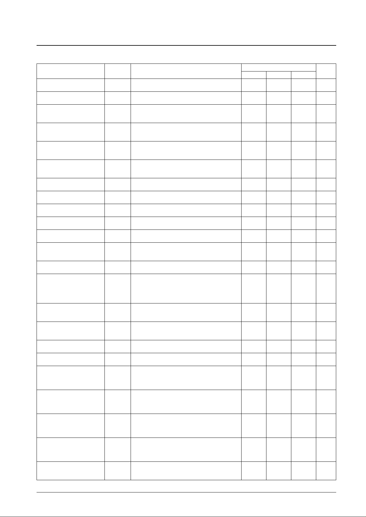
Continued from preceding page.
No. 4850-4/24
LA7265W
Parameter Symbol Conditions
Ratings
Unit
min typ max
γ.max characteristics 3 γM3
Measure the output voltage difference for inputs of
200 515 675 mV
0 Vp-p and 500 mVp-p. T5 output
γ.max knee characteristics γMK
Measure the output voltage difference for inputs of
520 750 930 mV
0 Vp-p and 1500 mVp-p. T5 output
Measure the output voltage difference for inputs of
γ dark clipping characteristics γMC 0 Vp-p and 200 mVp-p. Stipulated as the difference 0 105 280 mV
between that measurement and γM2. T5 output
Measure the output voltage difference for inputs of
Y gain control minimum gain γ2L 0 Vp-p and 200 mVp-p. Stipulated as the gain with –24 –16 –8 dB
respect to the input. T5 output
Measure the output voltage difference for inputs of
Y gain control maximum gain γ2H 0 Vp-p and 200 mVp-p. Stipulated as the gain with 10 11 12 dB
respect to the input. T5 output
Measure the output voltage difference for inputs of
Y gain control typical gain γ2T 0 Vp-p and 200 mVp-p. Stipulated as the gain with 0.2 1.4 2.3 dB
respect to the input. T5 output
Y gain control D range γ2D
Measure the output voltage difference for inputs of
1.10 1.53 V
0 Vp-p and 1500 mVp-p. T5 output
γ = 1 DC level γ2DC
Measure the output voltage (OPB) with no input.
0.87 1.49 2.11 V
T5 output
γ = 0.45 frequency characteristics γ1F
Stipulated as the gain difference between 10 MHz
–5.0 –3.8 dB
and f = 500 kHz. T5 output
γ = 1 frequency characteristics γ2F
Stipulated as the gain difference between 10 MHz
–2.9 –1.9 dB
and f = 500 kHz. T5 output
γ = 0.6 frequency characteristics γ3F
Stipulated as the gain difference between 10 MHz
–4.7 –3.7 dB
and f = 500 kHz. T5 output
Stipulated as the output voltage difference between
LSP.SW DC offset LSPDO SW14 being set to the B and A positions for a 0 Vp-p –10 0 +10 mV
input. T6 output
DL.OUT DC level LSPDC
Measure the output voltage (OPB) with no input.
2.30 2.52 2.75 V
T6 output
With SW14 in the B position, measure the output voltage
difference for inputs of 0 Vp-p and 500 mVp-p. Perform
LSP.SW gain differential LSPGD the same measurement with SW14 in the A position. –20 0 +20 mV
Stipulated as the difference between the two voltage
differences. T6 output
Measure the output voltage difference for inputs of
DL.OUT gain LSPG 0 Vp-p and 500 mVp-p. Stipulated as the gain with –0.5 0 +0.5 dB
respect to the input. T6 output
Input a f = 2 MHz, 200 mVp-p signal and adjust VR1 so
Aperture clipping standard voltage APCT that the output amplitude becomes 44 mVp-p. 2.35 2.60 2.85 V
Determine the VR9 voltage at that time. T7 output
Aperture clipping level (maximum) APCH
Measure the output for an f = 2 MHz, 200 mVp-p input
36 mV
signal. T7 output
Aperture maximum level APH
Measure the output for an f = 2 MHz, 200 mVp-p input
100 320 500 mV
signal. T7 output
Measure the output amplitude for an f = 2 MHz,
Aperture dark point APDP
200 mVp-p input signal. Stipulated as the VR4 setting
1.90 2.06 2.22 V
where the output starts to decrease when VR4 is slowly
increased starting at 0 mV. T7 output
With VR4 set at 0 V and 2.4 V, measure the output
Aperture dark slope (typical) APDST
gain for an f = 2 MHz, 200 mVp-p input signal.
–1.0 dB
Stipulated as the difference between those two gains.
T7 output
With VR4 set at 0 V and 2.4 V, measure the output
Aperture dark slope (minimum) APDSL
gain for an f = 2 MHz, 200 mVp-p input signal.
0.5 dB
Stipulated as the difference between those two gains.
T7 output
With VR4 set at 0 V and 2.4 V, measure the output
Aperture dark slope (maximum) APDSH
gain for an f = 2 MHz, 200 mVp-p input signal.
–4.0 dB
Stipulated as the difference between those two gains.
T7 output
Measure the output voltage difference for inputs of
Aperture Y signal gain APYG 0 Vp-p and 300 mVp-p. Stipulated as the gain with –1.0 –0.5 0 dB
respect to the input. T7 output
Continued on next page.
Page 5
Continued from preceding page.
No. 4850-5/24
LA7265W
Parameter Symbol Conditions
Ratings
Unit
min typ max
Aperture Y signal D range APYD
Measure the output voltage difference for inputs of
720 785 mV
0 Vp-p and 1200 mVp-p. T7 output
Aperture YOUT DC level APYDC
Measure the output voltage (OPB) with no input.
1.86 1.98 2.10 V
T7 output
Aperture YOUT frequency
APYF
Stipulated as the gain difference between 10 MHz
–7.2 –6.2 dB
characteristics and f = 500 kHz. T7 output
VIDEO-OUT DC level VODC
Measure (without setup) the pedestal voltage for
1.70 2.00 2.35 V
a 0 Vp-p input. T8 output
VIDEO-OUT sync level VOSY
Measure the pedestal and sink voltage difference for
500 550 630 mV
a 0 Vp-p input. T8 output
VIDEO-OUT typical pedestal level VOPT
Measure (without setup) the setup level for a 0 Vp-p
75 95 125 mV
input. T8 output
Measure the output voltage difference for inputs of
VIDEO-OUT gain VOG 0 Vp-p and 500 mVp-p. Stipulated as the gain with 7.30 7.75 8.20 dB
respect to the input. T8 output
VIDEO-OUT low clipping level VOLC
Measure the output voltage difference for inputs of
220 260 300 mV
0 Vp-p and –300 mVp-p. T8 output
VIDEO-OUT W.C. level (typical) VOWCT
Measure the output voltage difference for inputs of
1.42 1.50 1.58 V
0 Vp-p and 1200 mVp-p. T8 output
VIDEO-OUT minimum
VOPL Measure the setup level for a 0 Vp-p input. T8 output –180 –120 –80 mV
pedestal level
VIDEO-OUT maximum
VOPH Measure the setup level for a 0 Vp-p input. T8 output 180 240 280 mV
pedestal level
VIDEO-OUT W.C. level (maximum) VOWCH
Measure the output voltage difference for inputs of
0.85 0.93 1.00 V
0 Vp-p and 1200 mVp-p. T8 output
VIDEO-OUT D range VOD
Measure the output voltage difference for inputs of
1.80 2.03 V
0 Vp-p and 1200 mVp-p. T8 output
VIDEO-OUT frequency
VOF
Stipulated as the gain difference between f = 10 MHz
–3 –2 dB
characteristics and f = 500 kHz. T8 output
Measure the output voltage difference for inputs of
Aperture VIDEO-OUT linearity VOL
0 Vp-p and 100 mVp-p and the output voltage
98 %
difference for inputs of 400 mVp-p and 500 mVp-p.
Stipulated as the ratio of those two gains. T8 output
CDS current drain ICDS T10 output 5.50 7.85 10.20 mA
Video system current drain IVDO T11 and T15 outputs 16.5 23.5 30.5 mA
75 Ω driver current drain IDRI T12 output 4 6 8 mA
V
REF
reference voltage V
REF
T13 output 1.73 1.80 1.87 V
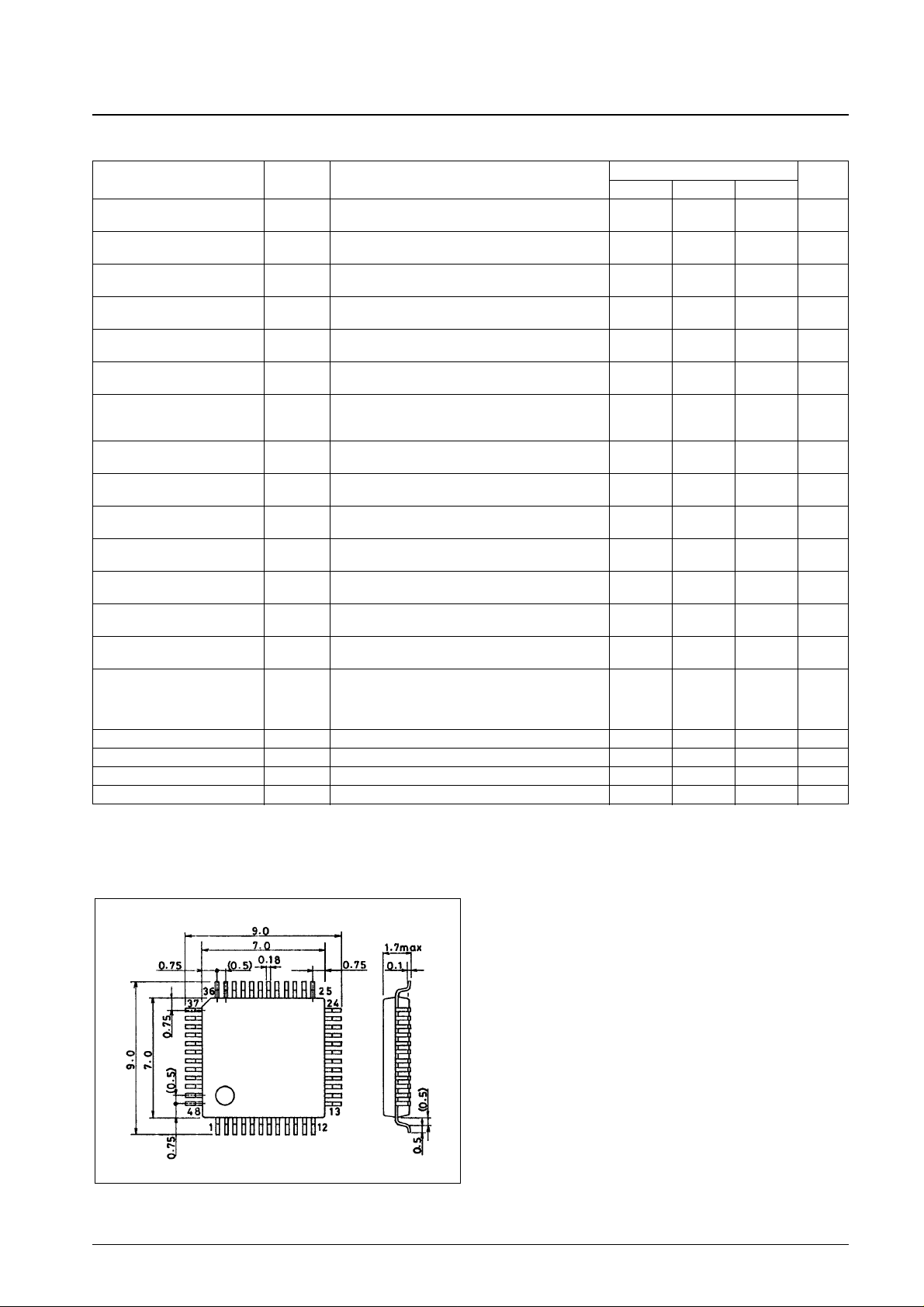
Package Dimensions
unit: mm
3163A-SQFP48
SANYO: SQFP48
[LA7265W]
Page 6
Switch Conditions
[CDS System]
[IRIS Amplifier System]
[AGC Amplifier System]
No. 4850-6/24
LA7265W
Symbol Input signal
Input pulse Trimmer voltage Switch
S2 S3 S4 S5 VR4 VR5 SW19 SW2 SW1
CCLIPH S1 = SIG.1 P1 P2 P3 P1 0 V 0 V B On On
CCLIPM S1 = SIG.1 P1 P2 P3 P1 0 V 0 V Off On On
CCLIPL S1 = SIG.1 P1 P2 P3 P1 0 V 0 V A On On
CDSD S1 = SIG.2 P1 P4 P5 5 V DC — — B — Off
CDSH S1 = SIG.1 P1 P6 P7 P1 0 V 0 V B On On
CDSO No signal P1 P2 P3 P1 0 V 0 V B On On
CDSN S1 = SIG.3 P1 P2 P3 P1 0 V 0 V B On On
CDSL S1 = SIG.1 P1 P2 P3 P1 0 V 0 V B On On
Symbol Input signal
Input pulse Trimmer voltage Switch
S2 S3 S4 S5 VR4 VR5 SW19 SW2
AGCDC1 No signal P1 P2 P3 P1 5 V 5 V B On
AGCHG1 S1 = SIG.1 P1 P2 P3 P1 5 V 5 V B On
AGCHG2 S1 = SIG.1 P1 P2 P3 P1 5 V — B Off
AGCHG3 S1 = SIG.1 P1 P2 P3 P1 5 V 0 V B On
AGCDC2 No signal P1 P2 P3 P1 0 V 0 V B On
AGCLG S1 = SIG.1 P1 P2 P3 P1 0 V 0 V B On
AGCLD S1 = SIG.1 P1 P2 P3 P1 5 V 5 V B On
AGCWC S1 = SIG.1 P1 P2 P3 P1 5 V 5 V B On
AGCT S1 = SIG.1 P1 P2 P3 P1 Scan — B Off
AGCF S1 = SIG.4 P1 P2 P8 P1 AGCT — B Off
AGCL S1 = SIG.1 P1 P2 P3 P1 AGCT — B Off
Symbol Input signal
Input pulse Switch
S2 S3 S4 S5 S6 SW19 SW3
IRISDC No signal P1 P2 P3 P1 P8 B Off
IRISP No signal P1 P2 P3 P1 P8 B Off
IRISWL S1 = SIG.1 P1 P2 P3 P1 P8 B B
IRISG S1 = SIG.1 P1 P2 P3 P1 P8 B A
IRISD S1 = SIG.1 P1 P2 P3 P1 P8 B A
IRSIWT S1 = SIG.1 P1 P2 P3 P1 P8 B Off
Page 7
[AGC Detector System]
[γ Correction System]
No. 4850-7/24
LA7265W
Input pulse
Trimmer
Switch
Symbol Input signal
voltage
S5 S6 VR6 SW5 SW4 SW6
CLP2L S8 = SIG.5 P1 P8 — — B, A Off
DETDC No signal P1 P8 — Off B Off
DETP No signal P1 P8 — Off B Off
DETWL S8 = SIG.5 P1 P8 — B A Off
DETG S8 = SIG.5 P1 P8 — A A Off
DETD S8 = SIG.5 P1 P8 — A A Off
DETWT S8 = SIG.5 P1 P8 — Off A Off
CONT1 No signal P1 5 V 1.4 V Off B On
CONT2 No signal P1 5 V 1.9 V Off B On
CONT3 No signal P1 5 V 2.4 V Off B On
Symbol Input signal
Input pulse Trimmer voltage Switch
S5 S6 VR2 VR3 SW4 SW7 SW8 SW9
γ1DC No signal P1 P8 0 V — B On Off Off
γ11 S8 = SIG.5 P1 P8 0 V — A On Off Off
γ12 S8 = SIG.5 P1 P8 0 V — A On Off Off
γ13 S8 = SIG.5 P1 P8 0 V — A On Off Off
γ1K S8 = SIG.5 P1 P8 0 V — A On Off Off
γ1P S8 = SIG.5 P1 P8 0 V — B On Off Off
γ1L S8 = SIG.5 P1 P8 0 V — A On Off Off
γ3DC No signal P1 P8 — 2.54 V B Off Off On
γ31 S8 = SIG.5 P1 P8 — 2.54 V A Off Off On
γ32 S8 = SIG.5 P1 P8 — 2.54 V A Off Off On
γ33 S8 = SIG.5 P1 P8 — 2.54 V A Off Off On
γ3K S8 = SIG.5 P1 P8 — 2.54 V A Off Off On
γM1 S8 = SIG.5 P1 P8 4 V 2.32 V A On Off On
γM2 S8 = SIG.5 P1 P8 4 V 2.32 V A On Off On
γM3 S8 = SIG.5 P1 P8 4 V 2.32 V A On Off On
γMK S8 = SIG.5 P1 P8 4 V 2.32 V A On Off On
γMC S8 = SIG.5 P1 P8 4 V 2.32 V A On On On
γ2L S8 = SIG.5 P1 P8 5 V 1.0 V A On Off On
γ2H S8 = SIG.5 P1 P8 5 V 5 V A On Off On
γ2T S8 = SIG.5 P1 P8 5 V — A On Off On
γ2D S8 = SIG.5 P1 P8 5 V 3.4 V A On Off On
γ2DC No signal P1 P8 5 V — B On Off Off
γ1F S8 = SIG.6 P1 P8 0 V — A On Off Off
γ2F S8 = SIG.6 P1 P8 5 V — A On Off Off
γ3F S8 = SIG.6 P1 P8 — 2.54 V A Off Off On
Page 8
[1H Interpolation: Aperture Correction System]
[Video Output System: Current Drain]
No. 4850-8/24
LA7265W
Input
Trimmer voltage Switch
Symbol Input signal
pulse
S7 VR4 VR1 SW10 SW11 SW12 SW14 SW15 SW16 SW13
LSPDO No signal P1 — — B Off — B, A — — —
LSPDC No signal P1 — — B Off — B — — —
LSPGD S10 = SIG.5 P1 — — A Off — B, A — — —
LSPG S10 = SIG.5 P1 — — A Off — B — — —
APCT S10 = SIG.6 P1 0 V Scan A A A B Off C Off
APCH S10 = SIG.6 P1 0 V — A A A B Off A Off
APH S10 = SIG.6 P1 0 V — A A A B Off B Off
APDP S10 = SIG.6 P1 Scan APCT A A A B A C Off
APDST S10 = SIG.6 P1 0, 2.4 V APCT A A A B Off C Off
APDSL S10 = SIG.6 P1 0, 2.4 V APCT A A A B B C Off
APDSH S10 = SIG.6 P1 0, 2.4 V APCT A A A B A C Off
APYG S10 = SIG.5 P1 — — A B B B — — Off
APYD S10 = SIG.5 P1 — — A B B B — — Off
APYDC No signal P1 — — B B B B — — Off
APYF S10 = SIG.6 P1 — — A B B B — — Off
Input pulse
Trimmer
Switch
Symbol Input signal
voltage
S2 S5 S7 S9 S11 VR12 SW6, 7 SW10 SW11 SW12 SW14 SW13 SW17 SW18
VODC S13 = SIG.5 — — P1 P9 P8 — — — — — — A Off Off
VOSY S13 = SIG.5 — — P1 P9 P8 — — — — — — A Off Off
VOPT S13 = SIG.5 — — P1 P9 P8 — — — — — — A Off Off
VOG S13 = SIG.5 — — P1 P9 P8 — — — — — — A Off Off
VOLC S13 = SIG.5 — — P1 P9 P8 — — — — — — A Off Off
VOWCT S13 = SIG.5 — — P1 P9 P8 — — — — — — A Off Off
VOPL S13 = SIG.5 — — P1 P9 P8 — — — — — — A B Off
VOPH S13 = SIG.5 — — P1 P9 P8 — — — — — — A A Off
VOWCH S13 = SIG.5 — — P1 P9 P8 — — — — — — A Off B
VOD S13 = SIG.5 — — P1 P9 P8 — — — — — — A Off A
VOF S13 = SIG.6 — — P1 P9 P8 — — — — — — A Off Off
VOL S13 = SIG.5 — — P1 P9 P8 — — A B B B B Off Off
ICDS No signal P1 — — — — — — — — — — — — —
IVDO No signal P1 P1 P1 — — 0 V On — B B — — — —
IDRI No signal — — — — — — — — — — — — — —
V
REF
No signal P1 P1 P1 — — — — — — — — — — —
Page 9

Pin Assignment and Equivalent Circuit Block Diagram
No. 4850-9/24
LA7265W
Page 10

Pin Functions
Unit (resistance: Ω), I: input, O: output, B: I/O, P: power supply
No. 4850-10/24
LA7265W
Pin No. Symbol I/O Equivalent circuit Function
1
2
3
4
5
6
CCD. IN
SH-GND
SH-D
VIDEO-V
CC
1
MAX. GAIN
CLP. C
I
P
I
P
I
B
CCD signal input. This pin can handle CCD signal reset levels up to
0.5 Vp-p. The data level is sliced at a maximum saturation output of
1.5 V.
CDS system ground. This line should be kept as short as possible
since the CDS system handles high frequencies.
This pin controls the charge and discharge speeds of the SH1 circuit.
Leave this pin open when a CCD element with 300,000 or fewer
pixels is used. Set this pin to 5 V when a CCD element with over
300,000 pixels is used.
AGC amplifier system V
CC
. Apply 5 V to this pin. Use pin 43 as the
corresponding ground. Either decouple (we recommend using a
power supply separate from the other V
CC
s for this voltage) or use a
DC-DC converter design so that signal component frequencies do
not leak into this V
CC
.
AGC maximum gain control.
The value of the maximum gain is:
About 15.5 dB when pin 5 is at 0 V,
About 24 dB when pin 5 is open, and
About 31 dB when pin 5 is at 5 V.
Charge/discharge capacitor used for post-CDS OPB clamping. We
recommend a value of 0.1 µF for this capacitor.
Continued on next page.
Page 11

Continued from preceding page.
Unit (resistance: Ω), I: input, O: output, B: I/O, P: power supply
No. 4850-11/24
LA7265W
Pin No. Symbol I/O Equivalent circuit Function
7
8
9
10
11
AGC. GAIN
AGC. CONT
DETECT. IN
DETECT. OUT
AGC. REF
I
O
I
O
I
AGC control signal input. The signal that was clamped by the postCDS OPB is split into two paths. The first path goes to the AGC
amplifier system. This pin is provided to adjust the AGC gain
according to the brightness, and it uses the smoothed AGC control
voltage output from pin 8. The AGC minimum gain is about –2 dB.
See the description of pin 39 for the second path from this pin.
AGC control signal output. This output is smoothed by an RC circuit
and then input to pin 7. The range over which the AGC control
voltage varies is about 1 to 3 V.
AGC detector circuit input. The pin 10 output is resistor divided,
smoothed and input to this pin.
AGC detector circuit output. A signal that has had pedestal added
and has been white clipped (see the pin 35 description) is amplified
by the AGC detector amplifier and output from this pin. An emitter
open circuit is used for this output. This output must be resistor
divided and smoothed by a capacitor.
AGC control amplifier reference input. The voltage input to pin 9 goes
to the AGC control amplifier. The state of this pin adjusts the AGC
control voltage. (This pin is normally left open.) If the image is too
bright, lower the AGC amplifier gain sensitivity by lowering this pin
(AGC.REF) to lower the AGC control voltage. If the image is too
dark, increase the AGC amplifier gain sensitivity by raising this pin
(AGC.REF) to increase the AGC control voltage.
Continued on next page.
Page 12

Continued from preceding page.
Unit (resistance: Ω), I: input, O: output, B: I/O, P: power supply
No. 4850-12/24
LA7265W
Pin No. Symbol I/O Equivalent circuit Function
12
13
14
15
V
REF
Y1. OUT
Y1. IN
GAMMA
O
O
I
I
1.8 V reference voltage. This pin outputs the OPB clamping
reference voltage used by pins 14, 23, 24 and 29. Insert a capacitor
between this pin and ground to stabilize this voltage.
Output for the signal amplified by the AGC circuit.
The signal that passed through the AGC amplifier is input to this pin
through a low-pass filter and a coupling capacitor. OPB clamping is
applied at the input stage. This clamping is applied with the timing of
the clamping pulse input to pin 41. The clamping level is about 1.8 V,
and when the OPB level is 1.8 V signals and noise with a level of
under about 0.5 V must not be input. If signals or noise at such levels
occur, or if pedestal displacement occurs at pin 23, (both of these
condition occur when the AGC maximum gain is at its maximum
level) first low clip the signal by inserting an NPN emitter follower at
pin 13, and then insert a low-pass filter. Use a low-pass filter with an
input impedance ratio of 1:10.
Gamma circuit selection and gamma variation control. The signal
OPB clamped at pin 14 is divided into two paths. The first path goes
to the gamma correction system. First, this signal is blanked with the
timing of the pre-blanking pulse input to pin 39 and pedestal is added
by a built-in DC source with a level essentially identical to the OPB
level. At that time, low clipping is applied at a level about 300 mV or
more below the OPB level. Next, the signal passes through the γ
correction circuit. However, there are three γ-correction circuits, one
with γ = 0.45, one with γ= 1, and one with a variable γ. The gamma
correction circuit is selected by this pin.
Pin 15 = 0 V:........................The γ= 0.45 circuit is used.
Pin 15 = 1 to 4 V:.................The variable γcircuit is used.
(When pin 15 is open:..........The variable γ circuit at γ = 0.6 is used.)
Pin 15 = 5 V:........................The γ= 1 circuit is used.
To select the maximum γ for the variable γ circuit, set the pin 15
voltage to 4 V. See the description of pin 35 for the second signal
path
Continued on next page.
Page 13

Continued from preceding page.
Unit (resistance: Ω), I: input, O: output, B: I/O, P: power supply
No. 4850-13/24
LA7265W
Continued on next page.
Pin No. Symbol I/O Equivalent circuit Function
16
17
18
19
20
PED. CLIP
Y. GAIN
VIDEO-V
CC
2
AP. DARK. SL
AP. CLIP
I
I
P
I
I
S-curve gamma control. This pin is normally left open when the
variable γ circuit is used. However, S-curve γ correction can be
enabled by clipping near the pedestal level by applying 5 V to this pin.
Y signal gain control. The signal that has passed through one of the
γ correction circuits goes to the Y gain control amplifier. This pin
adjusts the amount of amplification, which determines the amplitude
of the final output. This pin is normally left open when the γ = 0.45 or
the γ = 1 circuits are used. Gamma correction is applied when the
data level of the input CCD signal is under 500 mV, and the knee
characteristics apply when that level is over 500 mV. Set up pin 15
as follows to set the Y gain control output level for a 500 mV input
signal to be identical for all three gamma correction circuits.
When pin 15 is open (γ = 0.6): .......Pin 17 = 2.54 V
When pin 15 = 4 V (γ = max): ........Pin 17 = 2.32 V
Video system V
CC
. This VCCis used as the VCCfor all systems
except the CDS system, the AGC amplifier system and the 75 Ω
driver system. Apply 5 V and insert a 0.1 µF capacitor between this
pin and ground.
Aperture dark slope control. The aperture clipping level varies with
the AGC control voltage (pin 7). The clipping level is fixed for
relatively bright situations, i.e., when pin 7 is under 2 V. However, as
the image begins to get darker (i.e., as the pin 7 voltage moves from
about 2 V to the aperture dark point) the clipping level begins to
increase. When the AGC control voltage exceeds the aperture dark
point, the aperture is suppressed for low illumination and the clipping
level increases along with the AGC control voltage. It is this pin that
controls the coefficient for that increase.
Pin 19 = 0 V:........................Minimum coefficient value
Pin 19 = open: .....................Typical coefficient value
Pin 19 = 5 V:........................Maximum coefficient value
Aperture clipping control. The LA7265W clips the aperture whisker
components at the base. This pin adjusts the clipping level. Adjust
this pin if the IC internal slice level is inappropriate.
Page 14

Continued from preceding page.
Unit (resistance: Ω), I: input, O: output, B: I/O, P: power supply
No. 4850-14/24
LA7265W
Continued on next page.
Pin No. Symbol I/O Equivalent circuit Function
21
22
23
24
25
PED
W. CLIP
Y2. OUT
Y2. IN
Y2D. IN
I
I
O
I
I
Setup control. The setup level can be controlled by using this pin to
control the level of the pedestal that is added with the timing of the
blanking pulse input to pin 38.
Pin 21 = 0 V:........................Setup level = –120 mV
Pin 21 = open: .....................Setup level = 95 mV
Pin 21 = 5 V:........................Setup level = 240 mV
Saturation level control. The LA7265W white clips the signal to which
pedestal has been added at pin 21. This pin adjusts the white
clipping level.
Pin 22 = 0 V:........................Clipping at about 0.9 V
Pin 22 = open: .....................Clipping at about 1.5 V
Pin 22 = 5 V:........................Clipping at about 2.0 V
Outputs the signal that has passed through the Y gain control. (See
the description of pin 17.) Normally, this output is input to pin 24 (25)
through a coupling capacitor. However, it is input to pin 29 through a
coupling capacitor when aperture correction is not used.
Original signal input. Input the γ corrected signal through a coupling
capacitor. OPB clamping is applied at the input stage, clamping at
about 1.8 V. The clamping pulse signal is input to pin 40.
Input for the 1H delayed signal used for interpolation. When a low
resolution CCD device (e.g., about 60,000 pixels) is used and 1H
interpolation is desired, use a 1H delay line and input the 1H delayed
signal through a coupling capacitor. OPB clamping is applied at the
input stage, clamping at about 1.8 V. Leave this pin open when 1H
interpolation is not required. Input the clamping pulse signal to pin 40.
Page 15

Continued from preceding page.
Unit (resistance: Ω), I: input, O: output, B: I/O, P: power supply
No. 4850-15/24
LA7265W
Continued on next page.
Pin No. Symbol I/O Equivalent circuit Function
26
27
28
29
30
31
DL. OUT
DL. IN
Y3. OUT
Y3. IN
DRIVE-GND
VIDEO-OUT
B
I
O
I
P
O
Output to the delay line and input for the delay line reflected signal.
Outputs the signal that has passed through 1H interpolation. Aperture
correction is performed by inserting an aperture correction delay line
(with an impedance of about 1 kΩ) at this output. Since a 1 kΩ
resistor is built in to this pin's internal circuit, the DL reflected signal is
created at about 1/2 the level of the original signal. This signal is
combined with the original signal and the combination is input to the
aperture correction circuit.
Delay line delayed signal input. This pin inputs the signal that has
passed through the aperture correction delay line to the aperture
correction circuit. The combined signal consisting of the original
signal and the reflected signal is subtracted from the delay line signal
(pin 27), and the aperture whisker components are created by
amplifying that difference signal. See the description of pins 19 and
20 for details on whisker component control.
The aperture clipped whisker components are added to the original
signal at a fixed ratio and output from this pin. The original signal
gain is about 0 dB.
The aperture corrected signal is input to this pin through a coupling
capacitor. OPB clamping is applied at the input stage, clamping at
about 1.8 V with the timing of the clamp pulse signal input to pin 40.
Ground for the 75 Ω driver system.
Video signal output. A signal that has sync added at pin 37 and has
been amplified is output through the driver circuit. When output is to
a unit that has a 75 Ω load, the 140 IRE = about 1.9 V output signal
can be converted to a 140 IRE = about 1.0 V signal by inserting a
68 Ω resistor.
Page 16

Continued from preceding page.
Unit (resistance: Ω), I: input, O: output, B: I/O, P: power supply
No. 4850-16/24
LA7265W
Continued on next page.
Pin No. Symbol I/O Equivalent circuit Function
32
33
34
35
36
DRIVE-V
CC
IRIS-OUT
IRIS. WIN
AGC. WIN
LSP
P
O
I
I
I
75 Ω driver system V
CC
. Since the current variations in this system
are large, care must be taken to prevent this system from influencing
other power supplies. Apply a 5 V potential and insert a capacitor of
about 0.1 µF between this pin and ground.
Iris control signal output. The signal that had pedestal added and
was white clipped is amplified by about 10 dB by the iris amplifier and
output from this pin.
Iris window pulse input. White clipping is applied to the signal that
had pedestal added (see the pin 39 description). The clipping level
changes depending on this pin's input state. (0 V → maximum,
open → typical, 5 V → minimum clipping levels) Iris windowing is
possible by inputting an iris window pulse signal that has three
values: 0 V, floating, and 5 V.
AGC window pulse input. The other signal that had OPB clamping
applied at pin 14 goes to the AGC detector system. First a pedestal
on the order of a few tens of mV is added using the blanking pulse
input from pin 39. Next, white clipping is applied. However, the clipping
level changes according to the state of this pin. (0 V → maximum,
open → typical, 5 V → minimum clipping levels) AGC backlighting
correction is possible by inputting an AGC window pulse signal that
has three values: 0 V, floating, and 5 V.
1H interpolation control pulse input. When 1H interpolation is used,
input an LSP pulse ( ) that switches on each 1H to this pin. Pin
40 clamp pulse switching is performed by the LSP pulse. This circuit
also switches the OPB clamped original signal and the 1H delayed
signal. When 1H interpolation is not used, only the original signal is
OPB clamped and passed through this circuit.
Page 17

Continued from preceding page.
Unit (resistance: Ω), I: input, O: output, B: I/O, P: power supply
No. 4850-17/24
LA7265W
Continued on next page.
Pin No. Symbol I/O Equivalent circuit Function
37
38
39
40
41
C. CYNC
C. BLK
P. BLK
CLP2
CLP1
I
I
I
I
I
Composite synchronization signal pulse input. Sync is added to the
signal white clipped at pin 22 with the timing of the composite
synchronization pulse ( ) signal input to this pin. Also, the signal
including synchronization is amplified by about 7.7 dB. When the pin
29 input signal level is set to 500 mV (white average), the signal
level, including setup and sync, is amplified to be 140 IRE = about
1.9 V when pin 31 is unloaded. Therefore the pin 31 output will be:
White average: = about 1220 mV
Saturation level: = about 1700 mV (when the pin 29 input
saturation level is about 700 mV)
Sync level: = about 550 mV
Composite blanking pulse input. The signal OPB clamped at pin 24 is
blanked with the timing of the composite blanking pulse ( ) input
to this pin. Also, pedestal of the prescribed level is added with the
same timing and setup is also inserted. At that time, levels 250 mV or
more lower than the OPB level are low clipped.
Pre-blanking pulse input. The other path for the signal that was
clipped by the post-CDS OPB goes to the iris amplifier system. First,
pedestal is added using the pre-blanking pulse ( ) input to this
pin. In addition, this signal is also used by the AGC detector system
and the γ correction system.
Input for the output clamping pulse. This pin inputs the clamping
pulse ( ) for OPB clamping used by pins 24, 25 and 29. The
clamping pulse timing is delayed with respect to CLP1 to take into
account the amount the signal is delayed within the IC and by the
external LPF. When 1H interpolation is used, the clamping pulse is
turned on or off every 1H with the timing of the LSP pulse. This is
then used as the OPB clamp for pins 24 and 25.
OPB clamp pulse input. The dark current variations every 1H are
taken up by clamping, with the OPB timing, the signal that became a
continuous wave signal in the CDS system. This pin is the clamp
pulse ( ) input for that operation, and normally can be shared
with pin 42.
Page 18

Continued from preceding page.
Unit (resistance: Ω), I: input, O: output, B: I/O, P: power supply
No. 4850-18/24
LA7265W
Continued on next page.
Pin No. Symbol I/O Equivalent circuit Function
42
43
44
45
46
47
48
CLP0
VIDEO-GND
DS1
DS2
SH-V
CC
SH-P
SLICE
I
P
I
I
P
I
I
CCD signal clamp pulse input. The CCD signal input to pin 1 is
clamped to the prescribed voltage with the OPB timing. This pin inputs
that clamp pulse ( ), and normally can be shared with pin 41.
Ground for the video system.
Data timing sampling pulse input. This signal is divided into two paths
to perform CDS (correlation dual sampling) on the sliced CCD signal.
In the first path, the data level is sampled and held (SH1) with the
data timing. This pin is the sampling pulse ( ) input pin for that
function.
Pre-charge timing sampling pulse input. In the second sliced CCD
signal path, the precharge level is sampled and held (SH2) with the
precharge timing. This pin is the sampling pulse ( ) input pin for
that function. Next, this sampled and held signal is once again
sampled and held (SH3), here, by DS1 (the data timing sampling
pulse). Finally, the reset noise for each pixel is taken up by
subtracting these two sampled and held signals by a mixing amplifier.
CDS system VCC. Apply 5 V and insert a 0.1 µF capacitor between
this pin and ground.
This pin controls the charge/discharge speed of the SH2 and SH3
circuits. Pin usage is identical to that for pin 3.
CCD signal level control. Slices the saturation level of the CCD signal
that was OPB clamped. The possible slice levels are as follows:
Pin 48 = 0 V:........................about 1.5 V
Pin 48 = open: .....................about 1.1 V
Pin 48 = 5 V:........................about 0.5 V
Page 19

No. 4850-19/24
LA7265W
Page 20

Test Circuit
No. 4850-20/24
LA7265W
Page 21

Test Signals
No. 4850-21/24
LA7265W
Page 22

Test Input Pulse Signals
No. 4850-22/24
LA7265W
Page 23

No. 4850-23/24
LA7265W
Sample Application Circuit
Page 24

PS No. 4850-24/24
LA7265W
This catalog provides information as of September, 1998. Specifications and information herein are
subject to change without notice.
Specifications of any and all SANYO products described or contained herein stipulate the performance,
characteristics, and functions of the described products in the independent state, and are not guarantees
of the performance, characteristics, and functions of the described products as mounted in the customer’s
products or equipment. To verify symptoms and states that cannot be evaluated in an independent device,
the customer should always evaluate and test devices mounted in the customer’s products or equipment.
SANYO Electric Co., Ltd. strives to supply high-quality high-reliability products. However, any and all
semiconductor products fail with some probability. It is possible that these probabilistic failures could
give rise to accidents or events that could endanger human lives, that could give rise to smoke or fire,
or that could cause damage to other property. When designing equipment, adopt safety measures so
that these kinds of accidents or events cannot occur. Such measures include but are not limited to protective
circuits and error prevention circuits for safe design, redundant design, and structural design.
In the event that any or all SANYO products (including technical data, services) described or contained
herein are controlled under any of applicable local export control laws and regulations, such products must
not be exported without obtaining the export license from the authorities concerned in accordance with the
above law.
No part of this publication may be reproduced or transmitted in any form or by any means, electronic or
mechanical, including photocopying and recording, or any information storage or retrieval system,
or otherwise, without the prior written permission of SANYO Electric Co., Ltd.
Any and all information described or contained herein are subject to change without notice due to
product/technology improvement, etc. When designing equipment, refer to the “Delivery Specification”
for the SANYO product that you intend to use.
Information (including circuit diagrams and circuit parameters) herein is for example only; it is not
guaranteed for volume production. SANYO believes information herein is accurate and reliable, but
no guarantees are made or implied regarding its use or any infringements of intellectual property rights
or other rights of third parties.
 Loading...