

Page 1
Monolithic Linear IC
Ordering number : EN4896
63095HA (OT) No. 4896-1/9
SANYO Electric Co.,Ltd. Semiconductor Bussiness Headquarters
TOKYO OFFICE Tokyo Bldg., 1-10, 1 Chome, Ueno, Taito-ku, TOKYO, 110-8534 JAPAN
High-Fidelity Audio Signal Record/Playback
Processing Circuit for VCR Products
LA7256
Overview
The LA7256 provides the record and playback
amplification functions required for high-fidelity audio
signal processing in VCR systems. The record system
supports S-VHS and over-recording, and also supports the
provision of an adjustment-free record current by using a
constant-current regulated output scheme incorporating an
AGC circuit. The playback system consists of a high-gain
preamplifier with a small DC offset, and includes a builtin EP gain increasing function.
Functions
• Preamplifier (two channels)
• RF switching between CH1 and CH2
• Record AGC amplifier (for over-recording and S-VHS)
• Constant-current regulated output record amplifier
• Buffer amplifier that can be used in both record and
playback
Features
• Minimal number of required external components
• The playback amplifier output DC offset is small.
• Built-in EP mode gain emphasis
• Record AGC that handles three modes (for an
adjustment-free record current)
• Built-in buffer amplifier that can be used to construct an
active filter.
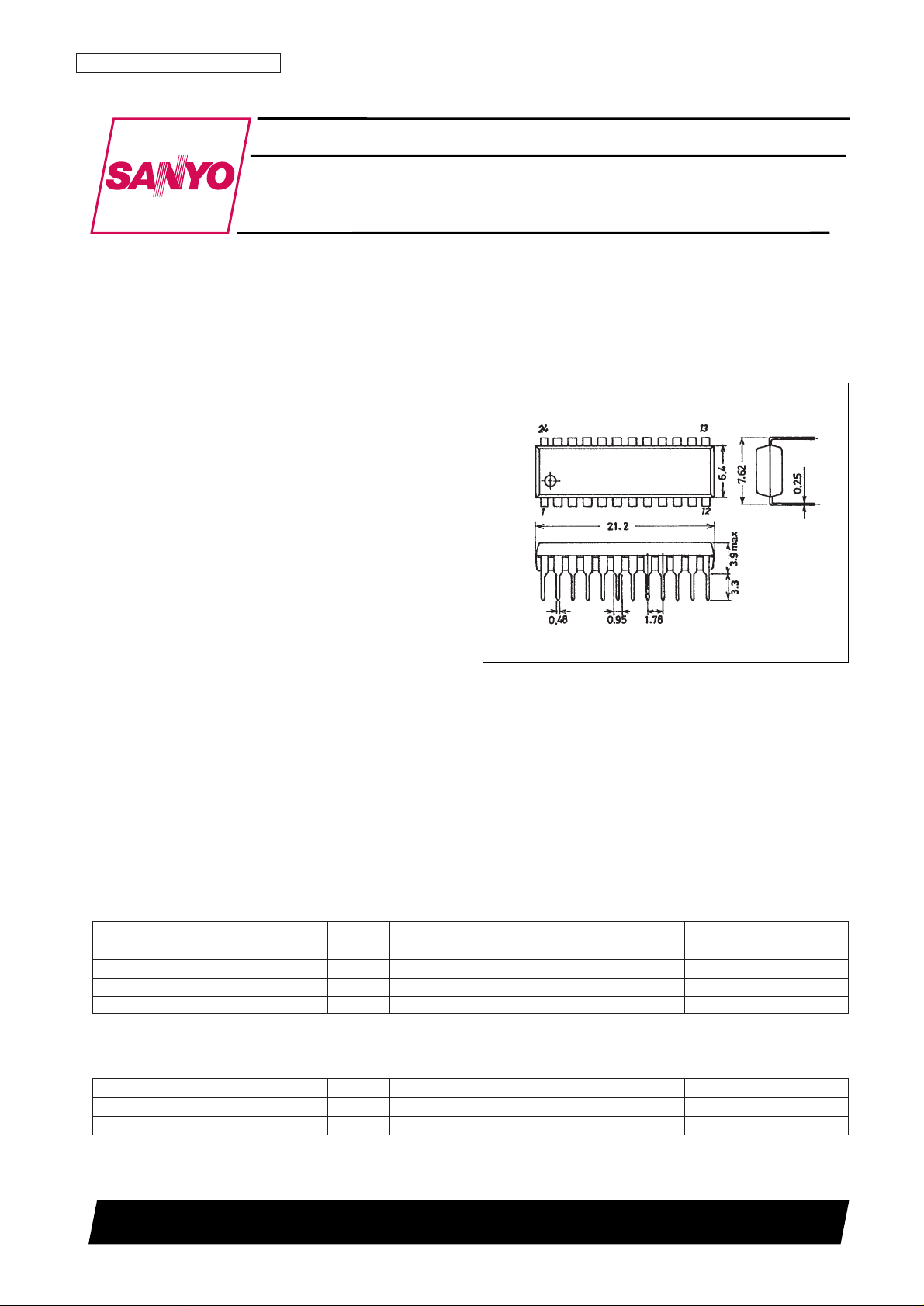
Package Dimensions
unit: mm
3067-DIP24S
Specifications
Maximum Ratings at Ta = 25°C
Operating Conditions at Ta = 25°C
Parameter Symbol Conditions Ratings Unit
Maximum supply voltage V
CC
max 7.0 V
Allowable power dissipation Pd max Ta ≤ 65°C 700 mW
Operating temperature Topr –10 to +65 °C
Storage temperature Tstg –55 to +150 °C
Parameter Symbol Conditions Ratings Unit
Recommended supply voltage V
CC
5.0 V
Operating supply voltage range V
CC
op 4.5 to 5.5 V
[LA7256]
SANYO: DIP24S
Page 2
Operating Characteristics at Ta = 25°C, VCC= 5 V, in the specified test circuit
Note: 1. Measure the input noise voltage after passing the pin 3 output (playback FM output) through a 1.1 MHz low-pass filter.
2. 1.3 MHz (70 mVp-p) + 1.7 MHz (180 mVp-p)
No. 4896-2/9
LA7256
Parameter Symbol Conditions min typ max Unit
[Playback Mode]
Circuit current I
CCP
No input: the pin 14 influx current 13 18 23 mA
Voltage gain, CH1 G
VP1
Pin 20 input = 100 µVp-p, f = 1.5 MHz, pin 1 = low:
72.5 75.5 78.5 dB
measure the pin 3 output.
Voltage gain, CH2 G
VP2
Pin 17 input = 100 µVp-p, f = 1.5 MHz, pin 1 = high:
72.5 75.5 78.5 dB
measure the pin 3 output.
Voltage gain difference ∆G
VP
G
VP1
– G
VP2
–2 0 2 dB
EP gain emphasis ∆G
EP
Pin 20 input = 100 µVp-p, f = 1.5 MHz, pin 1 = low:
1.7 2.4 3.1 dB
the ratio of the pin 3 outputs when pin 2 is high/low
Frequency characteristics, CH1 f
P1
Pin 20 input = 100 µVp-p, pin 1 = low: the difference
–3.0 –1.0 0 dB
in the levels on pin 3 when f = 2.2 MHz and 1.0 MHz
Pin 17 input = 100 µVp-p, f = 1.5 MHz, pin 1 = high:
Frequency characteristics, CH2 f
P2
the difference in the levels on pin 3 when f = 2.2 MHz –3.0 –1.0 0 dB
and 1.0 MHz
Pin 17 input = 0, pin 20 input = 100 µVp-p, f = 1.5 MHz:
Crosstalk CH1 to CH2 CT
1 → 2
the difference in the pin 3 output levels when pin 1 goes –40 –35 dB
from low to high
Pin 20 input = 0, pin 17 output = 100 µVp-p, f = 1.5 MHz:
Crosstalk CH2 to CH1 CT
2 → 1
the difference in the pin 3 output levels when pin 1 goes –40 –35 dB
from high to low
Equivalent input noise voltage CH1
V
NP1
With pin 20 grounded through 0.01 µF and 1 Ω,
0.8 1.0 µVrms
pin 1 = low: the pin 3 noise in input equivalent
*1
Equivalent input noise voltage CH2
V
NP2
With pin 17 grounded through 0.01 µF and 1 Ω,
0.8 1.0 µVrms
pin 1 = high: the pin 3 noise in input equivalent
*1
Second harmonic distortion CH1 2THD
1
Pin 20 input = 100 µVp-p, f = 1.5 MHz, pin 1 = low:
–50 –40 dB
the second harmonic in the pin 3 output
Second harmonic distortion CH2 2THD
2
Pin 17 input = 100 µVp-p, f = 1.5 MHz, pin 1 = high:
–50 –40 dB
the second harmonic in the pin 3 output
Maximum output voltage CH1 V
OMP1
With the pin 20 input varying, f = 1.5 MHz, pin 1 = low:
2.0 Vp-p
when the pin 3 third harmonic distortion is –30 dB
Maximum output voltage CH2 V
OMP2
With the pin 17 input varying, f = 1.5 MHz, pin 1 = high:
2.0 Vp-p
when the pin 3 third harmonic distortion is –30 dB
Pin 17 and 20 inputs = 0, pin 1 = low, pin 2 = low (SP):
Output DC offset 1 ∆V
ODC1
the difference in the pin 3 DC level when pin 1 goes –30 0 +30 mV
from low to high
Pin 17 and 20 inputs = 0, pin 1 = low, pin 2 = high (EP):
Output DC offset 2 ∆V
ODC2
the difference in the pin 3 DC level when pin 1 goes –50 0 +50 mV
from low to high
Head switching: CH1 hold voltage V
HS1
The pin 1 DC voltage required to operate CH1 0 1.0 V
Head switching: CH2 hold voltage V
HS2
The pin 1 DC voltage required to operate CH2 3.0 V
CC
V
Playback mode switch
R
SW
Calculate from the voltage difference on pin 16
4.0 6.0 Ω
on resistance when the pin 16 influx current is 1 mA and 2 mA.
SP hold voltage V
2
SP The pin 2 voltage required to hold SP mode 0 1.0 V
EP hold voltage V
2
EP The pin 2 voltage required to hold EP mode 3.0 V
CC
V
PB hold voltage V
5L
The pin 5 voltage required to hold PB mode 0 1.0 V
[Record Mode]
Circuit current I
CCR
No signal, the pin 14 influx current 45 63 81 mA
Output current I
OR
Pin 9 input = 180 mVp-p, f = 1.5 MHz:
48 53 58 mAp-p
measure the pin 16 output
AGC control characteristics 1 ∆V
AGC1
Pin 9 input = 90 and 180 mVp-p, f = 1.5 MHz:
–0.5 –0.2 dB
the ratio of the pin 16 output levels
AGC control characteristics 2 ∆V
AGC2
Pin 9 input = 360 and 180 mVp-p, f = 1.5 MHz:
0.2 0.5 dB
the ratio of the pin 16 output levels
Cross modulation distortion
CMD
04
For a pin 9 input*2, the 0.4 MHz spurious signal
–40 dB
0.4 MHz component in the pin 16 output current
Cross modulation distortion
CMD
09
For a pin 9 input*2, the 0.9 MHz spurious signal
–40 dB
0.9 MHz component in the pin 16 output current
Continued on next page.
Page 3
Continued from preceding page.
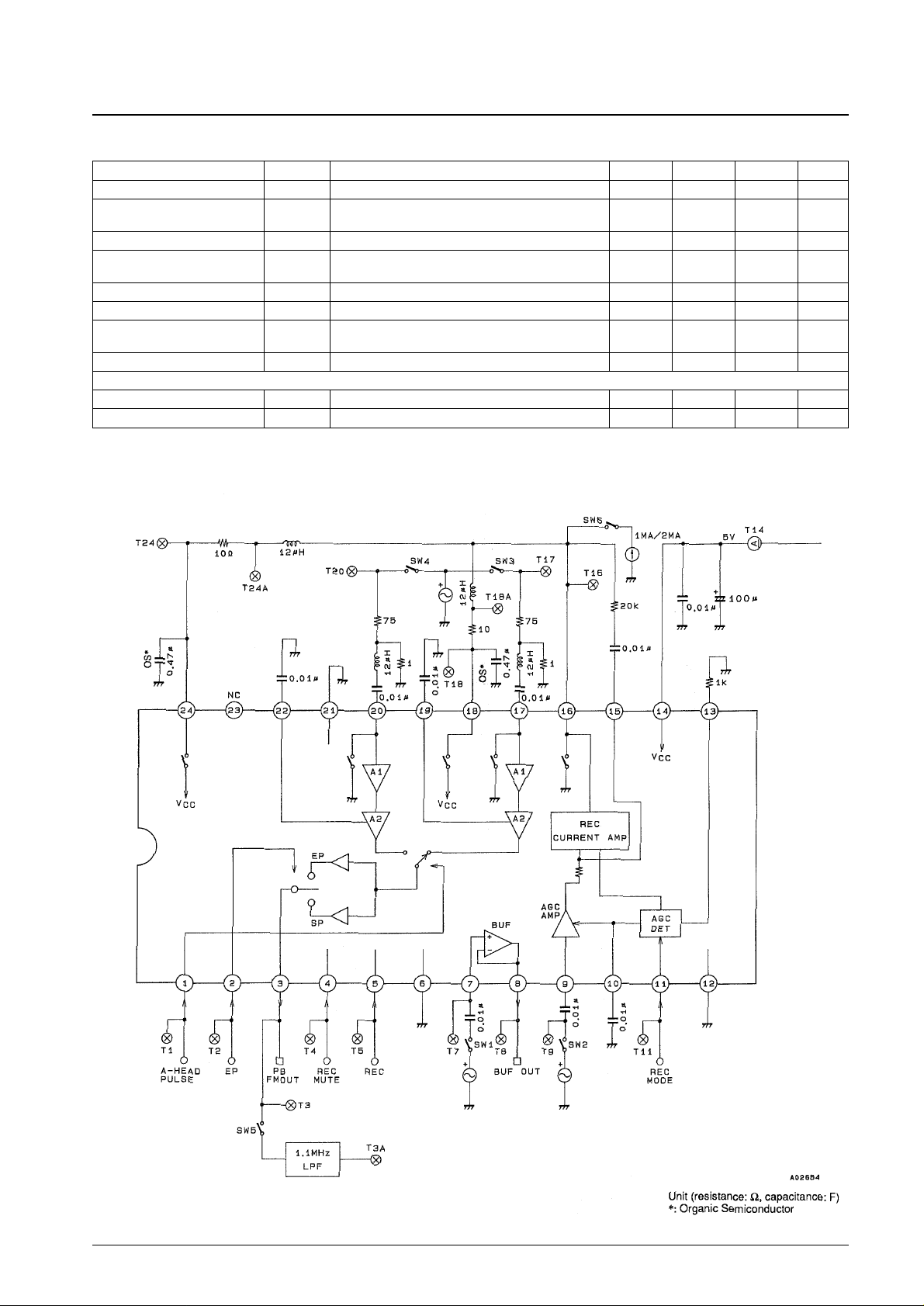
Test Circuit Diagram
No. 4896-3/9
LA7256
Parameter Symbol Conditions min typ max Unit
Over-record hold voltage V
11M
The pin 11 DC voltage for over-record mode 1.5 3.0 V
Over-record current ratio I
O-OV
Pin 9 input = 180 mVp-p, f = 1.5 MHz,
1.7 2.2 2.7 dB
pin 11 = middle level: measure the pin 16 output current
S-VHS hold voltage V
11H
The pin 11 DC voltage for S-VHS mode 3.5 V
CC
V
S-VHS current ratio I
O-SV
Pin 9 input = 180 mVp-p, f = 1.5 MHz, pin 11 = high:
–2.0 –2.6 –3.2 dB
measure the pin 16 output current
Record mute hold voltage 1 V
4L
The pin 4 DC voltage when record muting is off 0 1.0 V
Record mute hold voltage 2 V
4H
The pin 4 DC voltage when record muting is on 3.0 V
CC
V
Mute attenuation I
OR
, M
U
Pin 9 input = 180 mVp-p, f = 1.5 MHz, pin 4 = high:
–40 dB
measure the pin 16 output current
Record hold voltage V
5H
The pin 5 voltage required to hold record mode 3.0 V
CC
V
[Built-in Buffer]
Buffer I/O DC offset ∆V
BUF
–10 10 mV
Buffer frequency characteristics f
BUF
Pin 9 input = 180 mVp-p, f = 1/10 MHz –1 1 dB
Page 4

Application Circuit Block Diagram
No. 4896-4/9
LA7256
Page 5

Pin Functions
No. 4896-5/9
LA7256
Pin No. Symbol Pin internal equivalent circuit Function
1
2
3
4
5
6
A-HEAD PULSE
ES/SP
PB-FM OUT
REC MUTE
REC
GND
Low: 0 to 1.0 V → CH1
High: 3.0 to V
CC
→ CH2
Low: 0 to 1.0 V → SP
High: 3.0 to V
CC
→ EP
Low: 0 to 1.0 V → Mute off
High: 3.0 to V
CC
→ Mute on
Low: 0 to 1.0 V → PB
High: 3.0 to V
CC
→ REC
Ground for the playback output stage and record circuits
Continued on next page.
Page 6

Continued from preceding page.
No. 4896-6/9
LA7256
Pin No. Symbol Pin internal equivalent circuit Function
7
8
9
10
11
12
BUFF IN
BUFF OUT
REC FM IN
AGC FILT
REC MODE
REC OUT GND
DC voltage = 1/2 V
CC
Record amplifier input
Detects the record amplifier AGC detector output
Low: 0 to 1.0 V → Normal
Middle: 1.5 to 3.0 V → Over-record
High: 3.5 V to V
CC
→ S-VHS
Ground for the record output circuits
Continued on next page.
Page 7

Continued from preceding page.
No. 4896-7/9
LA7256
Pin No. Symbol Pin internal equivalent circuit Function
13
14
15
16
17
18
REC-CURR-ADJ
V
CC
REC BIAS
REC OUT
CH2-IN
PSW2
Converts the record output current output to a voltage.
Input block for the record current amplifier
Switch for record current output and playback mode on
On in PB mode
Playback amplifier CH2 input
CH2 head current supply
Continued on next page.
Page 8

No. 4896-8/9
LA7256
Continued from preceding page.
Pin No. Symbol Pin internal equivalent circuit Function
19
20
21
22
23
24
FILT2
CH1-IN
PB GND
FILT1
NC
PSW1
Generates the playback amplifier CH2 DC bias.
Playback amplifier CH1 input
Ground for the playback amplifier
Generates the playback amplifier CH1 DC bias.
Record amplifier CH2 head current supply
Page 9

PS No. 4896-9/9
LA7256
This catalog provides information as of June, 1995. Specifications and information herein are subject to change
without notice.
■ No products described or contained herein are intended for use in surgical implants, life-support systems, aerospace
equipment, nuclear power control systems, vehicles, disaster/crime-prevention equipment and the like, the failure of
which may directly or indirectly cause injury, death or property loss.
■ Anyone purchasing any products described or contained herein for an above-mentioned use shall:
➀ Accept full responsibility and indemnify and defend SANYO ELECTRIC CO., LTD., its affiliates, subsidiaries and
distributors and all their officers and employees, jointly and severally, against any and all claims and litigation and all
damages, cost and expenses associated with such use:
➁ Not impose any responsibility for any fault or negligence which may be cited in any such claim or litigation on
SANYO ELECTRIC CO., LTD., its affiliates, subsidiaries and distributors or any of their officers and employees
jointly or severally.
■ Information (including circuit diagrams and circuit parameters) herein is for example only; it is not guaranteed for
volume production. SANYO believes information herein is accurate and reliable, but no guarantees are made or implied
regarding its use or any infringements of intellectual property rights or other rights of third parties.
 Loading...