

Page 1
Any and all SANYO products described or contained herein do not have specifications that can handle
applications that require extremely high levels of reliability, such as life-support systems, aircraft’s
control systems, or other applications whose failure can be reasonably expected to result in serious
physical and/or material damage. Consult with your SANYO representative nearest you before using
any SANYO products described or contained herein in such applications.
SANYO assumes no responsibility for equipment failures that result from using products at values that
exceed, even momentarily, rated values (such as maximum ratings, operating condition ranges,or other
parameters) listed in products specifications of any and all SANYO products described or contained
herein.
Monolithic Linear IC
VCR Electronic Switch
Ordering number:ENN2834B
LA7221
SANYO Electric Co.,Ltd. Semiconductor Company
TOKYO OFFICE Tokyo Bldg., 1-10, 1 Chome, Ueno, Taito-ku, TOKYO, 110-8534 JAPAN
Overview
The LA7221 is an electronic switch that was designed for
use in audio video applications. It provides a wide dynamic
range. The LA7221 has on-chip video clamp circuits (clamp
elimination function).
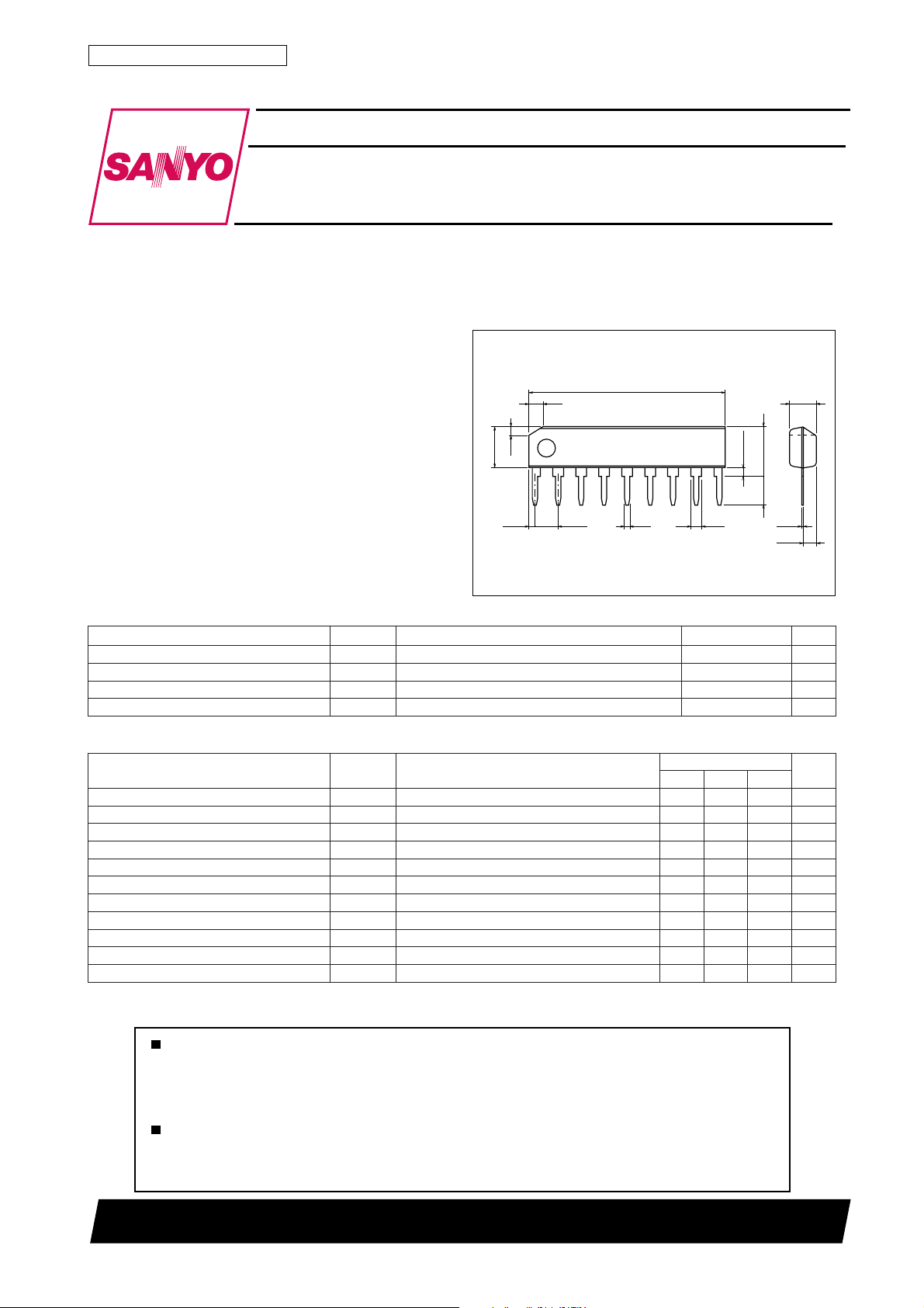
Package Dimensions
unit:mm
3017C-SIP9
[LA7221]
Features
1.5
22.3
• Low-voltage (5V) operation.
• Three inputs selectable and muting function.
• Video clamp circuits on chip.
4.8
1.0
• Wide dynamic range (2.0Vp-p or greater).
0.99
1
2.54
0.5
9
1.3
Specifications
Maximum Ratings at Ta = 25˚C
retemaraPlobmySsnoitidnoCsgnitaRtinU
egatlovylppusmumixaMV
noitapissidrewopelbawollAxamdP 001Wm
erutarepmetgnitarepOrpoT 07+ot01–
erutarepmetegarotSgtsT 521+ot04–
Operating Characteristics at Ta = 25˚C, VCC=5.0V
retemaraPlobmySsnoitidnoC
egatlovgnitarepOV
niardtnerruCI
leveltupnimumixaMV
citsiretcarahcycneuqerFG
noitrotsidcinomrahlatoTDHT 30.01.0%
klatssorCTC 07–06–Bd
tiucricgnitumnigniraeppaklatssorCTC
tesffoCDtuptuO
levelrevoegnahcLTCV
niaglaitnereffiDGD 5.00.1%
esahplaitnereffiDPD 5.00.1ged
xam 0.7V
CC
nimpytxam
po5.40.52.6V
CC
CC
xam0.22.2p-pV
NI
F
m
∆ TUOV
LTC
5.36.46.6Am
0.14.18.1V
0.51min
5.7max
3.2
0.25
1.35
SANYO : SIP9
sgnitaR
05.0±Bd
06–05–Bd
551Vm
3.0
˚C
˚C
tinU
42000TN (KT)/O3095MH/9058YT No.2834–1/3
Page 2
LA7221
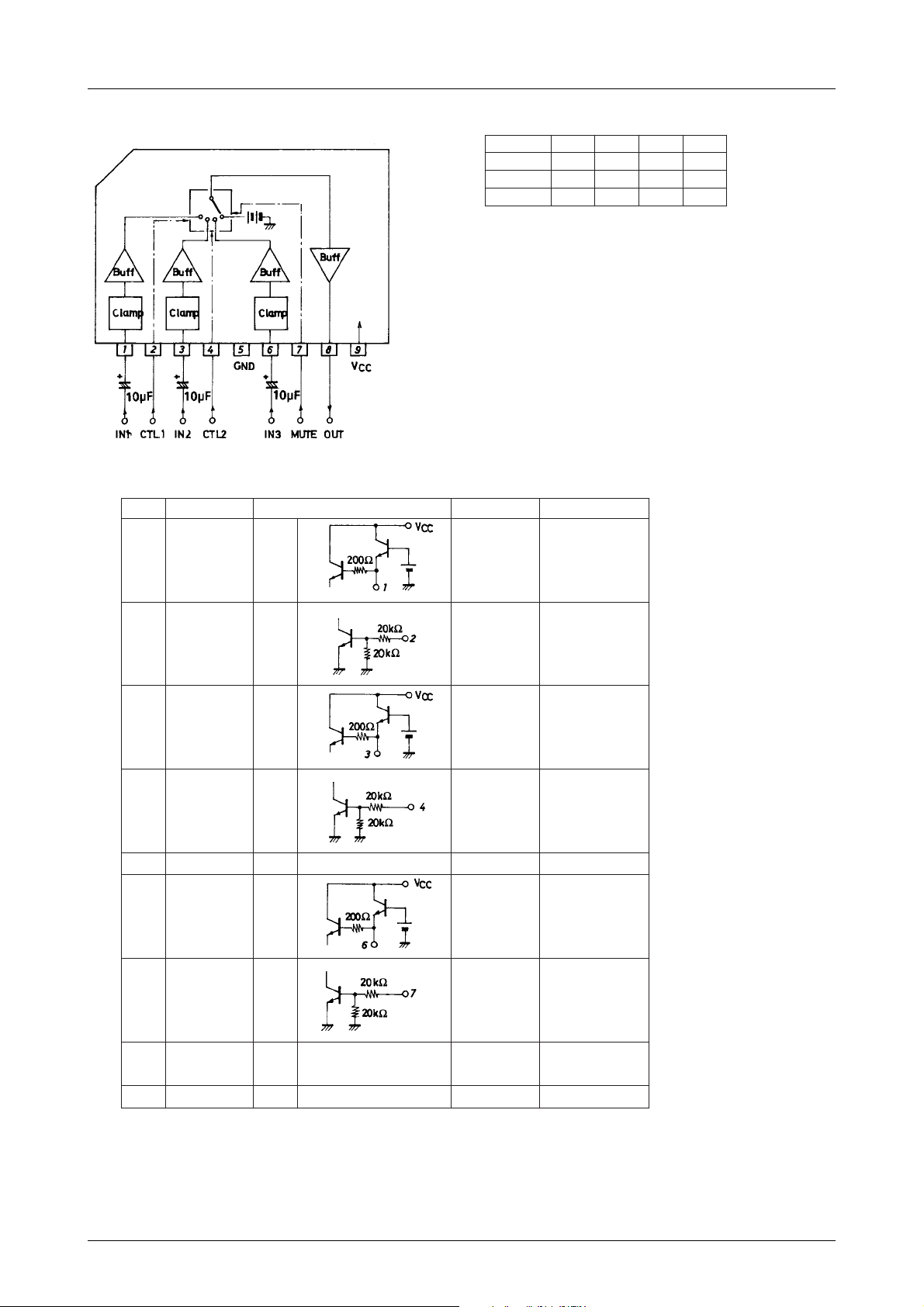
Block Diagram and Application Circuit Truth Table
1LTCHL–L
2LTCLH–L
LTCETUM LLHL
TUO1NI2NICD3NI
* : The output is indeterminate at other states
than shown above.
LA7221 Input / Output Configuration
niPemaNniPnoitarugifnoCO/IroecnadepmIO/IegatloVCDskrameR
11NI
21LORTNOCV0
32NI
42LORTNOCV0
5DNGV0
63NI
7
ETUM
∞
∞
∞
LORTNOC
V4.2
V0.2taNO
retaergro
V4.2
V0.2taNO
retaergro
V4.2
V0
V0.2taNO
retaergro
8TUO02 Ω rewollofrettimEV0.1
9V
CC
tnerrucrotcelloC
Am6.1
V0.5
No.2834–2/3
Page 3

LA7221
Specifications of any and all SANYO products described or contained herein stipulate the performance,
characteristics, and functions of the described products in the independent state, and are not guarantees
of the performance, characteristics, and functions of the described products as mounted in the customer's
products or equipment. To verify symptoms and states that cannot be evaluated in an independent device,
the customer should always evaluate and test devices mounted in the customer's products or equipment.
SANYO Electric Co., Ltd. strives to supply high-quality high-reliability products. However, any and all
semiconductor products fail with some probability. It is possible that these probabilistic failures could
give rise to accidents or events that could endanger human lives, that could give rise to smoke or fire,
or that could cause damage to other property. When designing equipment, adopt safety measures so
that these kinds of accidents or events cannot occur. Such measures include but are not limited to protective
circuits and error prevention circuits for safe design, redundant design, and structural design.
In the event that any or all SANYO products(including technical data,services) described or
contained herein are controlled under any of applicable local export control laws and regulations,
such products must not be exported without obtaining the export license from the authorities
concerned in accordance with the above law.
No part of this publication may be reproduced or transmitted in any form or by any means, electronic or
mechanical, including photocopying and recording, or any information storage or retrieval system,
or otherwise, without the prior written permission of SANYO Electric Co. , Ltd.
Any and all information described or contained herein are subject to change without notice due to
product/technology improvement, etc. When designing equipment, refer to the "Delivery Specification"
for the SANYO product that you intend to use.
Information (including circuit diagrams and circuit parameters) herein is for example only ; it is not
guaranteed for volume production. SANYO believes information herein is accurate and reliable, but
no guarantees are made or implied regarding its use or any infringements of intellectual property rights
or other rights of third parties.
This catalog provides information as of April, 2000. Specifications and information herein are subject to
change without notice.
PS No.2834–3/3
 Loading...