

SANYO LA7220 Datasheet
Ordering number: EN1409B
Monolithic Linear IC
LA7220
Electronic Switch for VCR/Audio Use
Overview
The LA7220 is a 3-channel 2-position high-performance analog
switch having wide application from audio band to video band.
It is also provided with 2 channels of muting function.
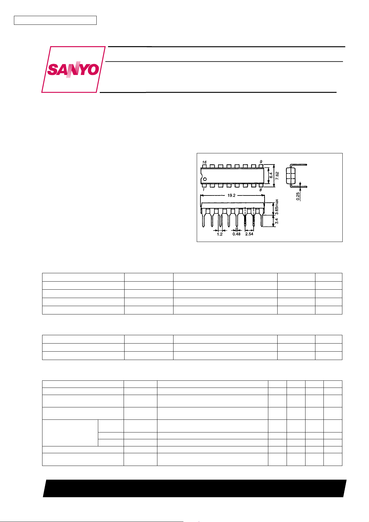
Package Dimensions
unit : mm
3006B-DIP16
[LA7220]
Features
.
3-channel 2-position switch
.
Wide input dynamic range
.
Low distortion
.
Good frequency characteristic
.
Muting available
SANYO : DIP16
Specifications
Maximum Ratings at Ta = 25°C
Parameter Symbol Conditions Ratings Unit
Maximum supply voltage V
Allowable power dissipation Pd max Ta % 65°C 500 mW
Operating temperature Topr –20 to +70 °C
Storage temperature Tstg –40 to +125 °C
max 15 V
CC
Operating Conditions at Ta = 25°C
Parameter Symbol Conditions Ratings Unit
Recommended supply voltage V
Operating voltage range V
CC
op 9to13 V
CC
Operating Characteristics at Ta = 25°C, VCC=12V
Parameter Symbol Conditions min typ max Unit
Current drain I
Total harmonic distortion THD
Noise voltage V
1ch CR1
Crosstalk
Pedestal level ∆Vped V
Maximum input voltage V
2ch CR2 Input 1: Rg = 50 Ω, (Note 2) –60 dB
3ch CR3 Input 1: Rg = 50 Ω, (Note 2) –50 dB
CC
NO
IN max
Rg = 600 Ω, 4.5 Vp-p,f=1kHz, R
(Note 1)
Rg = 600 Ω,f=20Hzto20kHz, RL= ∞,
(Note 1)
Input 1: Rg = 50 Ω, 2 Vp-p, f = 3.58 MHz,
Input 2: Rg = 500 Ω, (Note 2)
(Pins 10, 13, 15)=0to12V,(Note 1) –100
CTL
Rg = 600 Ω,f=1kHz, RL= ∞, THD = 1%,
(Note 1)
L
= ∞,
5.0 Vp-p
Continued on next page.
SANYO Electric Co.,Ltd. Semiconductor Bussiness Headquarters
TOKYO OFFICE Tokyo Bldg., 1-10, 1 Chome, Ueno, Taito-ku, TOKYO, 110 JAPAN
61096HA(II)/9068YT/8215KI,TS No.1409-1/6
12 V
30.0 39.9 mA
0.007 0.1 %
–93 –80 dBs
–50 dB
0 + 100
mV
LA7220
Continued from preceding page.
Parameter Symbol Conditions min typ max Unit
2nd harmonic voltage H2
3rd harmonic voltage H3
Switch changeover voltage V
Mute threshold voltage
Crosstalk between
channels
1ch
2ch –50 –68 dB
3ch –50 –68 dB
CTLS
V
ML
V
MH
Mute compression ratio
Control pin flow-in current I
Input impedance Z
Output impedance Z
(Pin 1) V
(Pin 2) V
(Pin 5) V
(Pin 6) V
(Pin 7) V
Pin voltage
(Pin 8) V
(Pin 9) V
(Pin 12) V
(Pin 16) V
CTL
IN
OUT
pin1
pin2
pin5
pin6
pin7
pin8
pin9
pin12
pin16
Note 1. Measurements are made for each of 1ch, 2ch, 3ch using input A and input B.
Input A: V
Input B: V
(pins 10, 13, 15) is 12 V at the measurement mode.
CTL
is 0 V at the measurement mode.
CTL
Rg=50Ω, 4.0 Vp-p,f=1MHz, R
(Note 1)
Rg=50Ω, 4.0 Vp-p,f=1MHz, R
(Note 1)
(Note 1) 2.6 3.1 4.0 V
Low level, (Note 3) 1.1 1.5 1.9 V
High level, (Note 3) 6.6 7.3 8.0 V
Rg = 500 Ω,R
Rg=50Ω, 2 Vp-p, f = 3.58 MHz, (Note 4)
=∞, other channel input
L
Rg = 600 Ω, 2 Vp-p,f=1kHz,
R
= ∞, series resistance 10 kΩ, (Note 3)
L
(Note 1) 8 µA
(Note 1) 10 kΩ
(Note 1) 29 Ω
V
=0V
pin15
V
= 12 V 7.9 V
pin15
Test point: V14
Test point: V2 7.2 V
V
=0V
pin13
V
= 12 V 7.9 V
pin13
Test point: V16
Test point: V5 7.2 V
Test point: V7 7.2 V
V
=0V
pin10
V
= 12 V 7.9 V
pin10
V
=0V
pin10
V
= 12 V 7.9 V
pin10
V
=0V
pin13
V
= 12 V 7.9 V
pin13
V
=0V
pin15
V
= 12 V 7.9 V
pin15
Test point: V18
Test point: V17
Test point: V15
Test point: V13
L
L
= ∞,
= ∞,
–46 –55 dB
–46 –55 dB
–50 –68 dB
–60 dB
7.9 V
7.9 V
7.9 V
7.9 V
7.9 V
7.9 V
2. Measurements are made using input A and B.
3. Measurements are made for 1ch, 3ch.
4. Measurements are made for each of 1ch, 2ch, 3ch using input A and B on other channels.
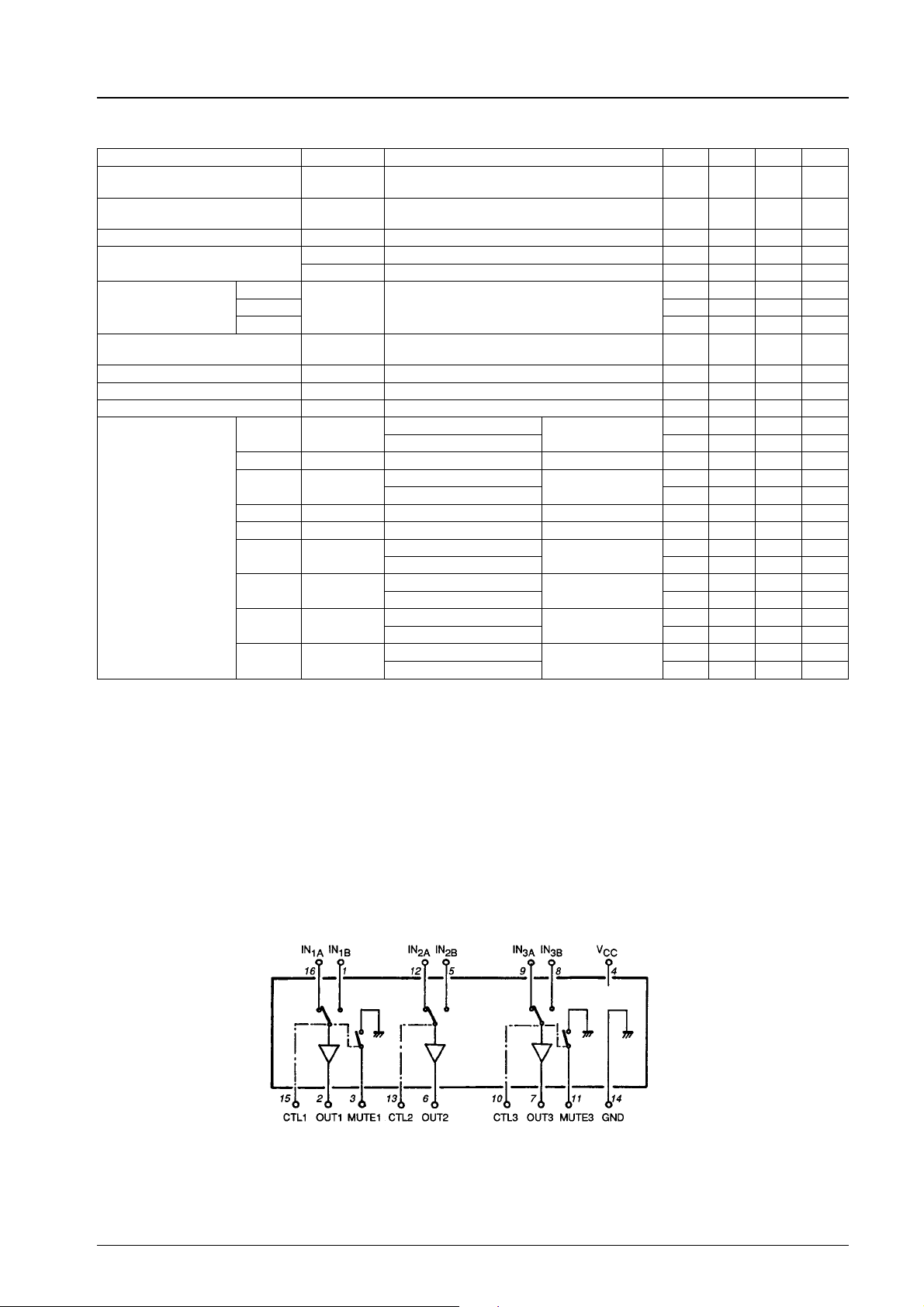
Equivalent Circuit Block Diagram
No.1409-2/6
 Loading...