

Page 1
Any and all SANYO products described or contained herein do not have specifications that can handle
applications that require extremely high levels of reliability, such as life-support systems, aircraft’s
control systems, or other applications whose failure can be reasonably expected to result in serious
physical and/or material damage. Consult with your SANYO representative nearest you before using
any SANYO products described or contained herein in such applications.
SANYO assumes no responsibility for equipment failures that result from using products at values that
exceed, even momentarily, rated values (such as maximum ratings, operating condition ranges,or other
parameters) listed in products specifications of any and all SANYO products described or contained
herein.
Monolithic Linear IC
UHF Band RF Modulator
Ordering number:ENN*5571
LA7172M
SANYO Electric Co.,Ltd. Semiconductor Company
TOKYO OFFICE Tokyo Bldg., 1-10, 1 Chome, Ueno, Taito-ku, TOKYO, 110-8534 JAPAN
Preliminary
Overview
The LA7172M is a monolithic IC for an RF modulator
which generates RF TV channel signal in UHF band, from
a baseband video and audio signal.
Audio FM carrier is controlled by PLL system and gener-
ated without L/C tank.
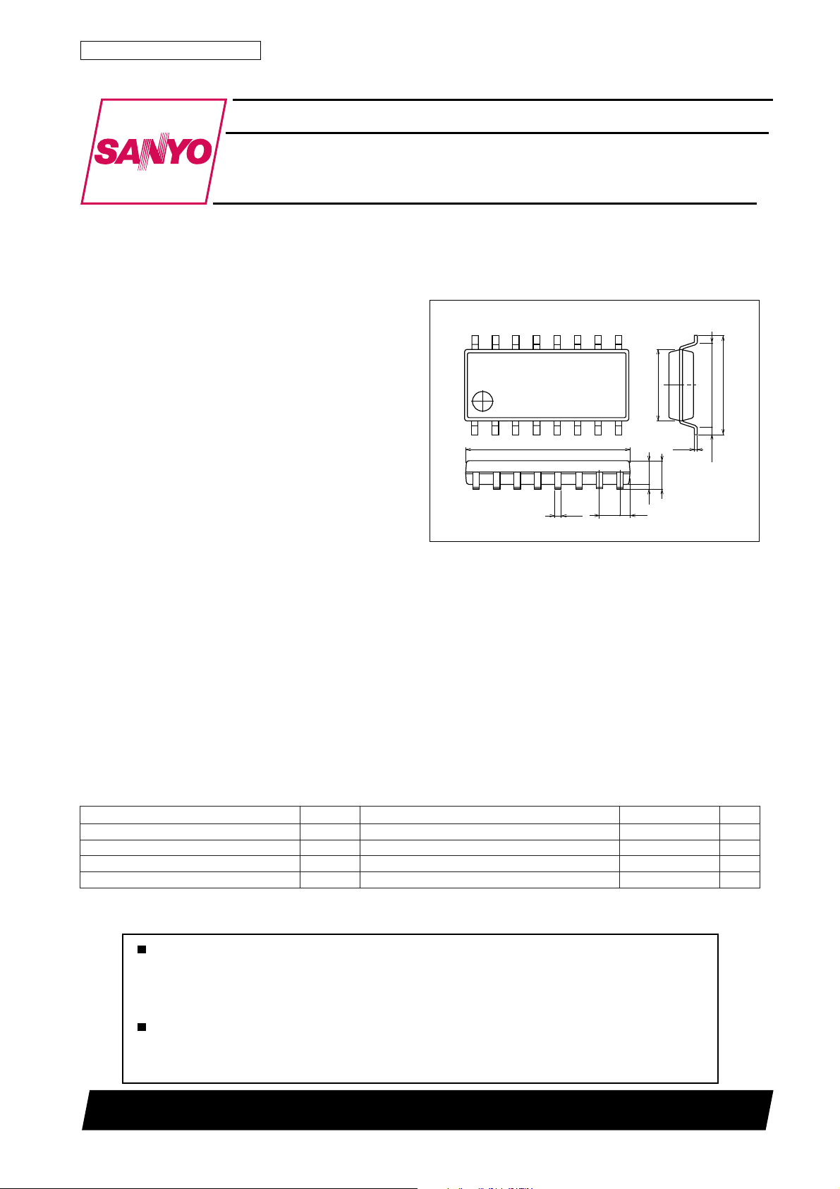
Package Dimensions
unit:mm
3035A-MFP16
[LA7172M]
16
9
Features
• 5V operation.
• Less supply current.
• Balanced RF VCO.
• Wide bandwidth.
• PLL controlled and tankless audio FM (4 sound
intercarrier frequency capability).
• Small package.
• Package : MFP16.
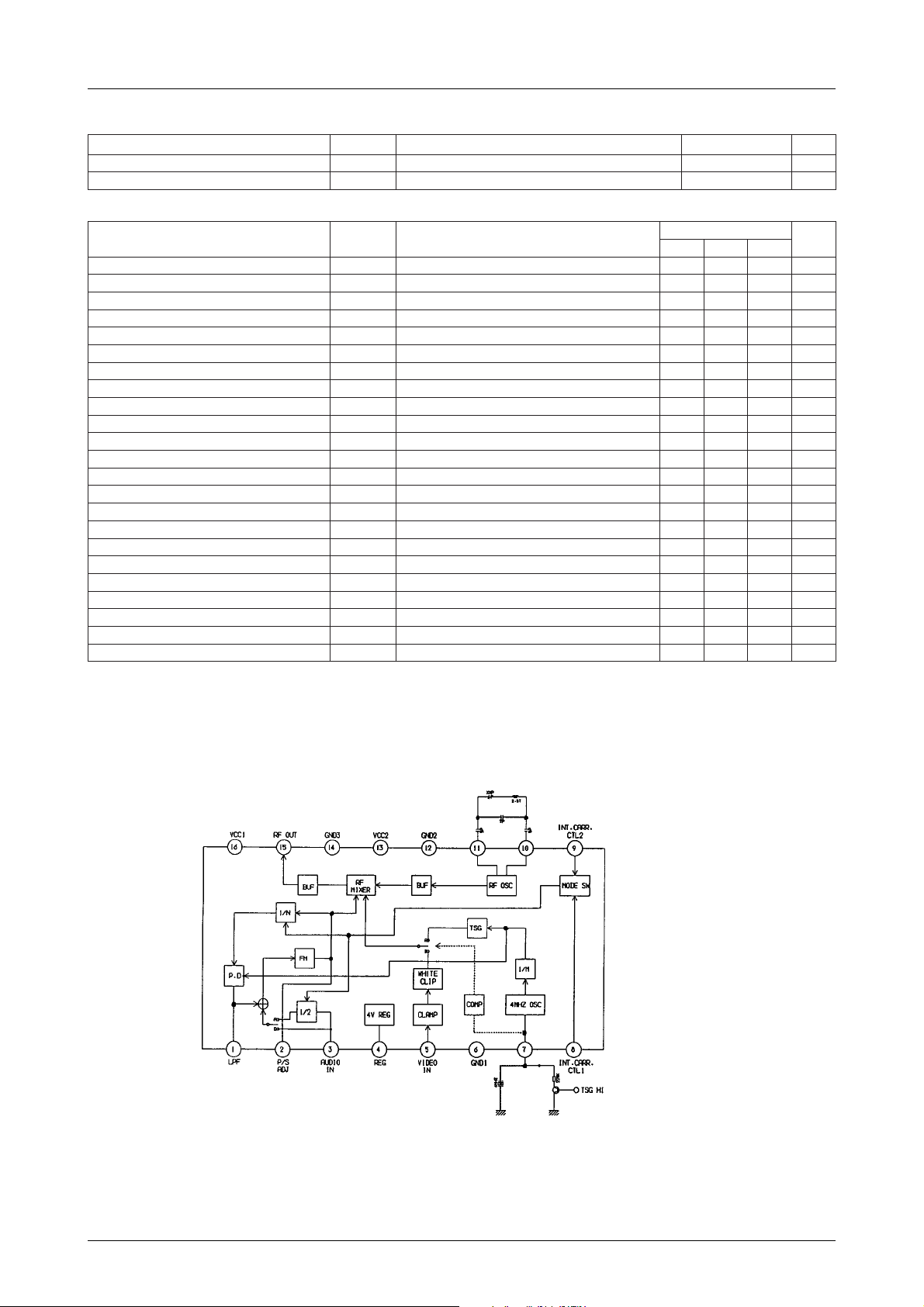
Functions
• RF VCO.
• V ideo modulator.
• Sound carrier converter.
• RF buffer.
• V ideo clamp.
• White clip.
• Audio FM.
• 4V regulator.
• Reference oscillatior.
• TSG (test signal generator).
Specifications
Maximum Ratings at Ta = 25˚C
retemaraPlobmySsnoitidnoCsgnitaRtinU
egatlovylppusmumixaMV
noitapissidrewopelbawollAxamdP 052Wm
erutarepmetgnitarepOrpoT 57+ot02–
erutarepmetegarotSgtsT 051+ot55–
xam 7V
CC
Ta≤75˚C
4.4
1
10.1
0.35
1.27
8
0.15
1.5
1.8max
0.1
0.605
SANYO : MFP16
5.15
0.625
6.4
˚C
˚C
42000TN (KT)/73196RM No.5571–1/3
Page 2
LA7172
Operating Conditions at Ta = 25˚C
retemaraPlobmySsnoitidnoCsgnitaRtinU
egatlovylppusdednemmoceRV
egatlovgnitarepOV
Operating Characteristics at Ta = 25˚C, VCC=5V
retemaraPlobmySsnoitidnoC
tnerrucylppuSI
egatlovrotalugeRgerVlangisoN7.39.31.4V
tuptuoFRPlangisoN775.9728µBd
oitarS/PS/P2+pf:S × zHM5.45.21515.71Bd
scinomrahdn2dnuoS2S/P2+pf:2S × zHMsf**Bd
scinomrahdr3dnuoS3S/P3+pf:3S × zHMsf**Bd
taebecnanimorhCBC/PV
scinomrahoediV2V/PV
noitaludomoediVpMV
levelpilcetihWLCWV
niaglaitnereffiDGDV
esahplaitnereffiDPDV
noitaludomGSTGSTpMhgih:7V070809%
oitarSVGSTS/V.cnys/oediv,hgih:7V7.3/3.62.3/8.67.2/3.7
doirepGSTSThgih:7V7.360.463.46sµ
htdiw.cnysGSTSHhgih:7V6.30.44.4sµ
htdiwetihwGSTH
esiretihwts1GST1VTesiretihwts1dna.cnysneewtebhtdiw,hgih:7V224262sµ
esiretihwdn2GST2VTesiretihwdn2dna.cnysneewtebhtdiw,hgih:7V830424sµ
noitaludomMFoiduAMFsMV
noitaludomoiduaxaMxmsM%3<DHT004%
DHTMFoiduAMFDHTVNIp-pV1,zHk1=35.02%
N/SMFoiduAMFN/SV
* : TBD
CC
po 5.5ot5.4V
CC
nimpytxam
CC
V
langisoN420363Am
NI
NI
NI
NI
NI
NI
hgih:7V6.30.44.4sµ
NI
NI
p-pV1,petsriatS=5370878%
p-pV1,petsriatS=55–5%
p-pV1,petsriatS=56–6geD
V,p-pV1,zHk1=3
NI
csf–sf+pf:BCp-pV4.0,csf=55657Bd
zHM2+pf:2Vp-pV1,zHM1=50526Bd
p-pV5.1,petsriatS=5883989%
%001:VEDzHk05±p-pV66.1,zHk1=309001011%
p-pV1,rabroloc=53455Bd
sgnitaR
5V
tinU
Note
fp : picture RF carrier, fs : sound intercarrier (B/G 5.5MHz), fsc : sub carrier (4.43MHz)
Equivalent Circuit Block Diagram
No.5571–2/3
Page 3

Sample Application Circuit
LA7172M
Specifications of any and all SANYO products described or contained herein stipulate the performance,
characteristics, and functions of the described products in the independent state, and are not guarantees
of the performance, characteristics, and functions of the described products as mounted in the customer's
products or equipment. To verify symptoms and states that cannot be evaluated in an independent device,
the customer should always evaluate and test devices mounted in the customer's products or equipment.
SANYO Electric Co., Ltd. strives to supply high-quality high-reliability products. However, any and all
semiconductor products fail with some probability. It is possible that these probabilistic failures could
give rise to accidents or events that could endanger human lives, that could give rise to smoke or fire,
or that could cause damage to other property. When designing equipment, adopt safety measures so
that these kinds of accidents or events cannot occur. Such measures include but are not limited to protective
circuits and error prevention circuits for safe design, redundant design, and structural design.
In the event that any or all SANYO products(including technical data,services) described or
contained herein are controlled under any of applicable local export control laws and regulations,
such products must not be exported without obtaining the export license from the authorities
concerned in accordance with the above law.
No part of this publication may be reproduced or transmitted in any form or by any means, electronic or
mechanical, including photocopying and recording, or any information storage or retrieval system,
or otherwise, without the prior written permission of SANYO Electric Co. , Ltd.
Any and all information described or contained herein are subject to change without notice due to
product/technology improvement, etc. When designing equipment, refer to the "Delivery Specification"
for the SANYO product that you intend to use.
Information (including circuit diagrams and circuit parameters) herein is for example only ; it is not
guaranteed for volume production. SANYO believes information herein is accurate and reliable, but
no guarantees are made or implied regarding its use or any infringements of intellectual property rights
or other rights of third parties.
This catalog provides information as of April, 2000. Specifications and information herein are subject to
change without notice.
PS No.5571–3/3
 Loading...